SNVSAR5B December 2016 – March 2018 LMR23625-Q1
PRODUCTION DATA.
- 1 Features
- 2 Applications
- 3 Description
- 4 Revision History
- 5 Device Comparison
- 6 Pin Configuration and Functions
- 7 Specifications
-
8 Detailed Description
- 8.1 Overview
- 8.2 Functional Block Diagram
- 8.3
Feature Description
- 8.3.1 Fixed-Frequency Peak-Current-Mode Control
- 8.3.2 Adjustable Output Voltage
- 8.3.3 EN/SYNC
- 8.3.4 VCC, UVLO
- 8.3.5 Minimum ON-Time, Minimum OFF-Time and Frequency Foldback at Dropout Conditions
- 8.3.6 Power Good (PGOOD)
- 8.3.7 Internal Compensation and CFF
- 8.3.8 Bootstrap Voltage (BOOT)
- 8.3.9 Overcurrent and Short-Circuit Protection
- 8.3.10 Thermal Shutdown
- 8.4 Device Functional Modes
-
9 Application and Implementation
- 9.1 Application Information
- 9.2
Typical Applications
- 9.2.1 Design Requirements
- 9.2.2
Detailed Design Procedure
- 9.2.2.1 Custom Design With WEBENCH® Tools
- 9.2.2.2 Output Voltage Setpoint
- 9.2.2.3 Switching Frequency
- 9.2.2.4 Inductor Selection
- 9.2.2.5 Output Capacitor Selection
- 9.2.2.6 Feed-Forward Capacitor
- 9.2.2.7 Input Capacitor Selection
- 9.2.2.8 Bootstrap Capacitor Selection
- 9.2.2.9 VCC Capacitor Selection
- 9.2.2.10 Undervoltage Lockout Setpoint
- 9.2.3 Application Curves
- 10Power Supply Recommendations
- 11Layout
- 12Device and Documentation Support
- 13Mechanical, Packaging, and Orderable Information
Package Options
Refer to the PDF data sheet for device specific package drawings
Mechanical Data (Package|Pins)
- DRR|12
- DDA|8
Thermal pad, mechanical data (Package|Pins)
Orderable Information
9.2.3 Application Curves
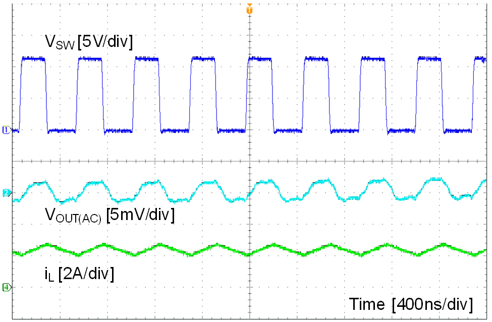
Unless otherwise specified the following conditions apply: VIN = 12 V, fSW = 2100 kHz, L = 2.2 µH, COUT = 47 µF, TA = 25°C.
| VOUT = 5 V | IOUT = 2.5 A | fSW = 2100 kHz |

| VOUT = 5 V | IOUT = 0 mA | fSW = 2100 kHz |

| VIN = 12 V | VOUT = 5 V | IOUT = 2 A |

| VIN = 12 V | VOUT = 5 V | IOUT = 0.2 A to 2.5 A, 100 mA / μs |

| VOUT = 5 V | IOUT = 2 A to short |

| VOUT = 5 V | IOUT = 100 mA | fSW = 2100 kHz |

| VOUT = 5 V | IOUT = 0 mA | fSW = 2100 kHz |

| VIN = 12 V | VOUT = 5 V | IOUT = 2 A |

| VOUT = 7 V to 36 V, 2 V / μs | VOUT = 5 V | IOUT = 2.5 A |

| VOUT = 5 V | IOUT = short to 2 A |