SNVS738H October 2011 – June 2019 LMR24210
PRODUCTION DATA.
- 1 Features
- 2 Applications
- 3 Description
- 4 Revision History
- 5 Pin Configuration and Functions
- 6 Specifications
-
7 Detailed Description
- 7.1 Overview
- 7.2 Functional Block Diagram
- 7.3
Feature Description
- 7.3.1 COT Control Circuit Overview
- 7.3.2 Start-up Regulator (VCC)
- 7.3.3 Regulation Comparator
- 7.3.4 Zero Coil Current Detect
- 7.3.5 Overvoltage Comparator
- 7.3.6 On-Time Timer, Shutdown
- 7.3.7 Current Limit
- 7.3.8 N-Channel Mosfet and Driver
- 7.3.9 Soft Start
- 7.3.10 Thermal Protection
- 7.3.11 Thermal Derating
- 8 Application and Implementation
- 9 Layout
- 10Device and Documentation Support
Package Options
Mechanical Data (Package|Pins)
- YPA|28
Thermal pad, mechanical data (Package|Pins)
Orderable Information
8.2.1.2 External Components
The following guidelines can be used to select external components.
RFB1 and RFB2: Choose these resistors from standard values in the range of 1 kΩ to 10 kΩ, satisfying the following ratio:
For VOUT = 0.8 V, the FB pin can be connected to the output directly with a pre-load resistor drawing more than 20 µA. This is needed because the converter operation needs a minimum inductor current ripple to maintain good regulation when no load is connected.
RON:Equation 2 can be used to select RON if a desired operating frequency is selected. But the minimum value of RON is determined by the minimum on-time. It can be calculated as follows:

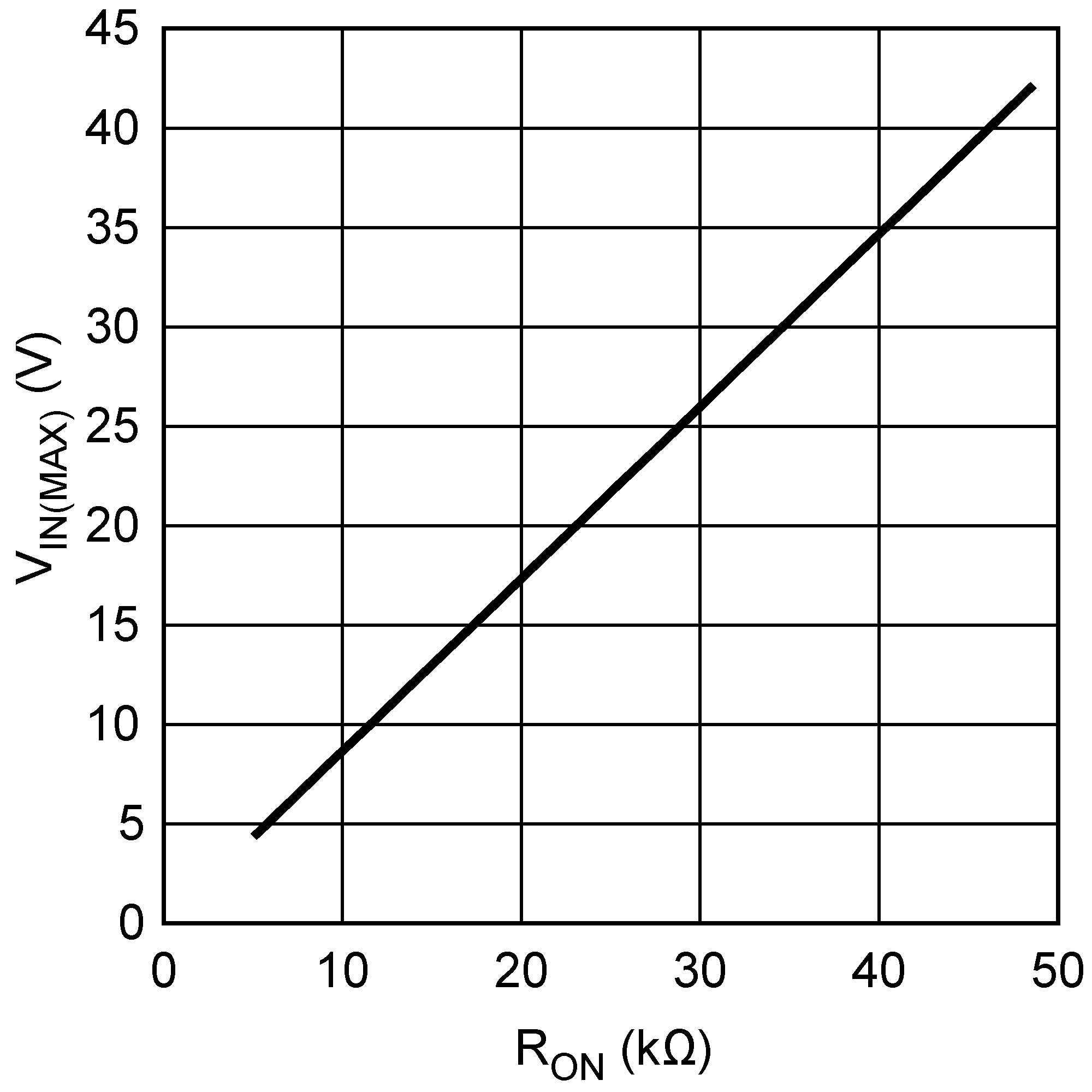
If RON calculated from Equation 2 is smaller than the minimum value determined in Equation 10, select a lower frequency to re-calculate RON by Equation 2. Alternatively, VIN(MAX) can also be limited in order to keep the frequency unchanged. The relationship of VIN(MAX) and RON is shown in Figure 22.
On the other hand, the minimum off-time of 260 ns can limit the maximum duty ratio.
 Figure 22. Maximum VIN For Selected RON
 L: The main parameter affected by the inductor is the amplitude of inductor current ripple (ILR). Once ILR is selected, L can be determined by:
If the output current IOUT is determined, by assuming that IOUT = IL, the higher and lower peak of ILR can be determined. Beware that the higher peak of ILR should not be larger than the saturation current of the inductor and current limits of the main and synchronous MOSFETs. Also, the lower peak of ILR must be positive if CCM operation is required.
 Figure 23. Inductor Selection for VOUT = 3.3 V
  Figure 24. Inductor Selection for VOUT = 0.8 V
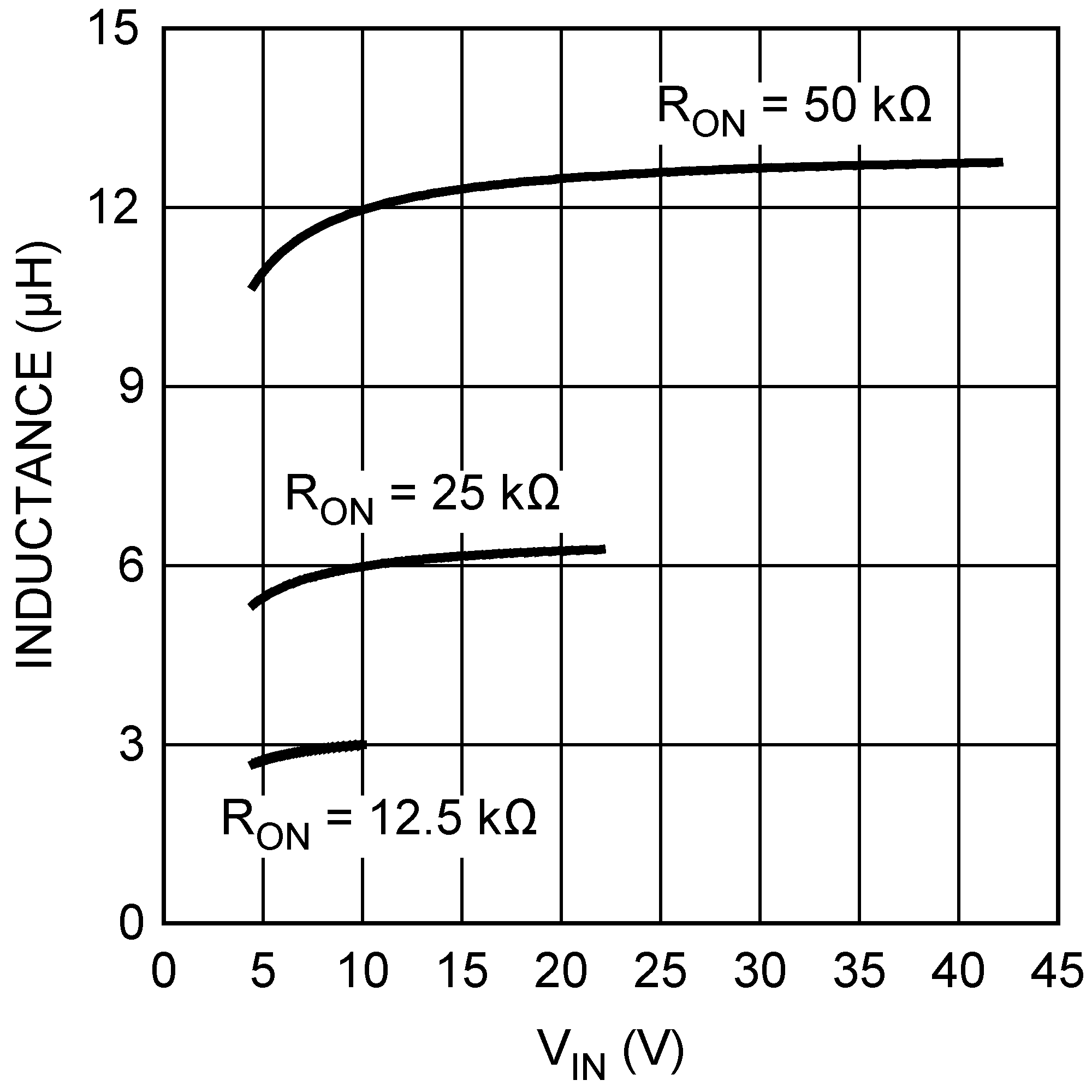
 Figure 23 and Figure 24 show curves on inductor selection for various VOUT and RON. For small RON, according to Equation 10, VIN is limited. Some curves are therefore limited as shown in the figures.
CVCC: The capacitor on the VCC output provides not only noise filtering and stability, but also prevents false triggering of the VCC UVLO at the main MOSFET on/off transitions. CVCC should be no smaller than 680 nF for stability, and should be a good quality, low ESR, ceramic capacitor.
COUT and COUT3: COUT should generally be no smaller than 10 µF. Experimentation is usually necessary to determine the minimum value for COUT, as the nature of the load may require a larger value. A load which creates significant transients requires a larger COUT than a fixed load.
COUT3 is a small value ceramic capacitor located close to the LMR24210 to further suppress high frequency noise at VOUT. TI recommends a 100-nF capacitor.
CIN and CIN3: The function of CIN is to supply most of the main MOSFET current during the on-time, and limit the voltage ripple at the VIN pin, assuming that the voltage source connecting to the VIN pin has finite output impedance. If the voltage source’s dynamic impedance is high (effectively a current source), CIN supplies the average input current, but not the ripple current.
At the maximum load current, when the main MOSFET turns on, the current to the VIN pin suddenly increases from zero to the lower peak of the inductor’s ripple current and ramps up to the higher peak value. It then drops to zero at turn-off. The average current during the on-time is the load current. For a worst case calculation, CIN must be capable of supplying this average load current during the maximum on-time. CIN is calculated from:

where
- IOUT is the load current
- ton is the maximum on-time
- ΔVIN is the allowable ripple voltage at VIN
The purpose of the CIN3 is to help avoid transients and ringing due to long lead inductance at the VIN pin. A low ESR 0.1-µF ceramic chip capacitor located close to the LMR24210 is recommended.
CBST: A 33-nF high-quality ceramic capacitor with low ESR is recommended for CBST since it supplies a surge current to charge the main MOSFET gate driver at turnon. Low ESR also helps ensure a complete recharge during each off-time.
CSS: The capacitor at the SS pin determines the soft-start time; that is, the time for the reference voltage at the regulation comparator and the output voltage to reach their final value. The time is determined from Equation 13:

CFB: If the output voltage is higher than 1.6 V, CFB is needed in the DCM to reduce the output ripple. The recommended value for CFB is 10 nF.
