SNVS738H October   2011  – June 2019 LMR24210

PRODUCTION DATA.  

  1. Features
  2. Applications
  3. Description
    1.     Device Images
      1.      Typical Application
  4. Revision History
  5. Pin Configuration and Functions
    1.     Pin Descriptions
  6. Specifications
    1. 6.1 Absolute Maximum Ratings
    2. 6.2 ESD Ratings
    3. 6.3 Recommended Operating Ratings
    4. 6.4 Electrical Characteristics
    5. 6.5 Typical Characteristics
  7. Detailed Description
    1. 7.1 Overview
    2. 7.2 Functional Block Diagram
    3. 7.3 Feature Description
      1. 7.3.1  COT Control Circuit Overview
      2. 7.3.2  Start-up Regulator (VCC)
      3. 7.3.3  Regulation Comparator
      4. 7.3.4  Zero Coil Current Detect
      5. 7.3.5  Overvoltage Comparator
      6. 7.3.6  On-Time Timer, Shutdown
      7. 7.3.7  Current Limit
      8. 7.3.8  N-Channel Mosfet and Driver
      9. 7.3.9  Soft Start
      10. 7.3.10 Thermal Protection
      11. 7.3.11 Thermal Derating
  8. Application and Implementation
    1. 8.1 Application Information
    2. 8.2 Typical Application
      1. 8.2.1 Detailed Design Procedure
        1. 8.2.1.1 Custom Design With WEBENCH® Tools
        2. 8.2.1.2 External Components
      2. 8.2.2 Application Curve
  9. Layout
    1. 9.1 Layout Considerations
    2. 9.2 Layout Examples
    3. 9.3 Package Considerations
  10. 10Device and Documentation Support
    1. 10.1 Device Support
      1. 10.1.1 Development Support
        1. 10.1.1.1 Custom Design With WEBENCH® Tools
    2. 10.2 Receiving Notification of Documentation Updates
    3. 10.3 Community Resources
    4. 10.4 Trademarks
    5. 10.5 Electrostatic Discharge Caution
    6. 10.6 Glossary

Package Options

Mechanical Data (Package|Pins)
Thermal pad, mechanical data (Package|Pins)
Orderable Information

Typical Characteristics

Unless otherwise specified all curves are taken at VIN = 18 V with the configuration in the typical application circuit for VOUT = 3.3 V (Figure 26) TA = 25°C.
LMR24210 30173804.png
Figure 1. VCC vs ICC
LMR24210 30173806.png
Figure 3. Ton vs VIN
LMR24210 30173808.png
Figure 5. VFB vs Temperature
LMR24210 30173870.gif
VOUT = 3.3 V
Figure 7. Efficiency vs Load Current
LMR24210 30173872.gif
Figure 9. Efficiency vs Load Current (VOUT = 0.8v)
LMR24210 30173876.gif
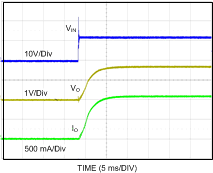
VOUT = 3.3 V, 1-A Loaded
Figure 11. Power Up
LMR24210 30173815.gif
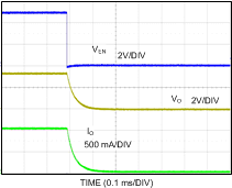
VOUT = 3.3 V, 1 A Loaded
Figure 13. Shutdown Transient
LMR24210 30173817.gif
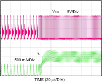
VOUT = 3.3 V, 0.5 A Loaded
Figure 15. Discontinuous Mode Operation
LMR24210 30173805.png
Figure 2. VCC vs VIN
LMR24210 30173875.gif
Figure 4. Switching Frequency, FSW vs VIN, VOUT=0.8v,
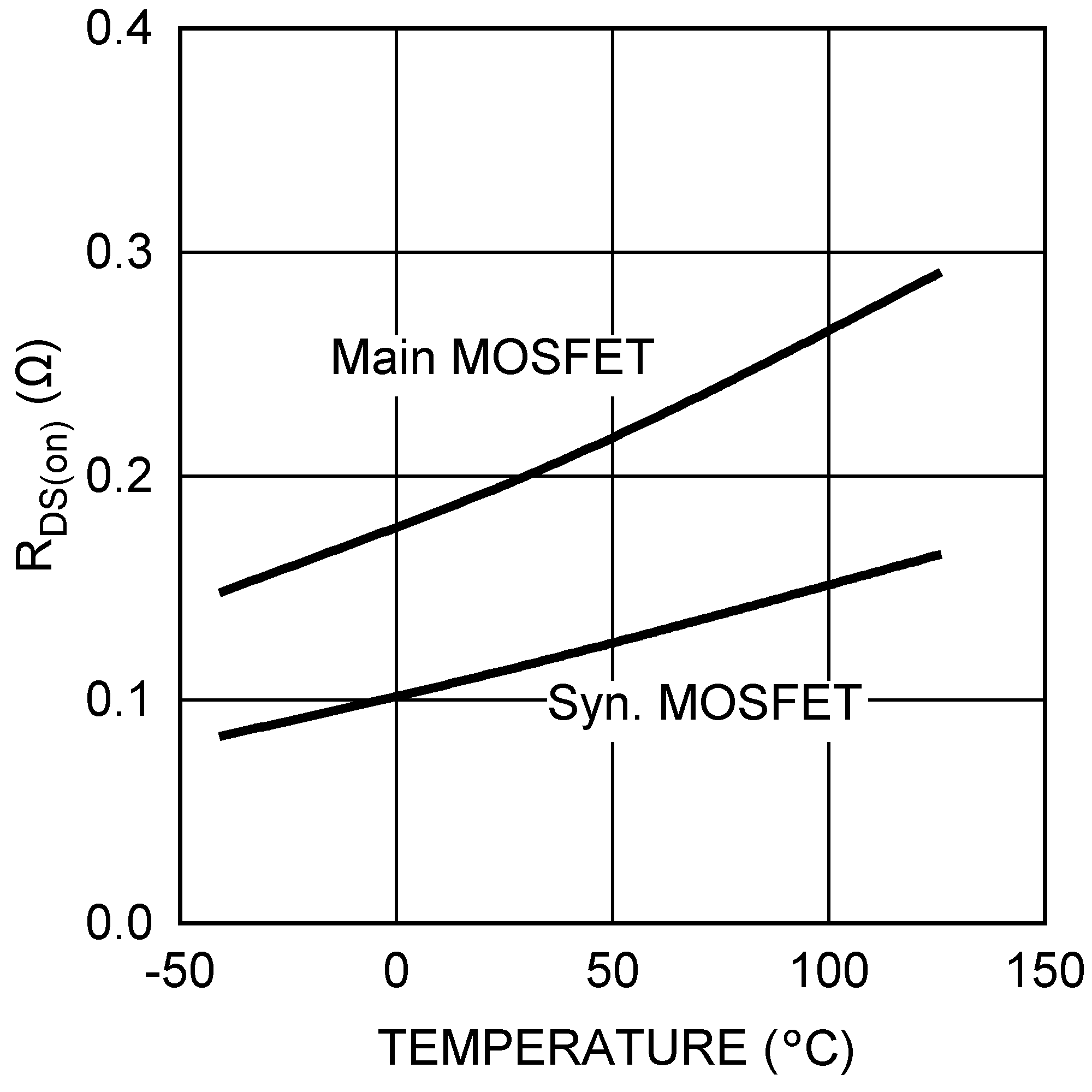
LMR24210 30173809.png
Figure 6. RDS(on) vs Temperature
LMR24210 30173871.gif
VOUT = 3.3 V
Figure 8. VOUT Regulation vs Load Current
LMR24210 30173873.gif
VOUT = 0.8 V
Figure 10. VOUT Regulation vs Load Current
LMR24210 30173814.gif
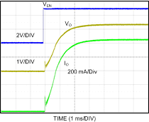
VOUT = 3.3 V, 1-A Loaded
Figure 12. Enable Transient
LMR24210 30173816.gif
VOUT = 3.3 V, 1 A Loaded
Figure 14. Continuous Mode Operation
LMR24210 30173818.gif
VOUT = 3.3 V, 0.5 A to 1 A Load
Figure 16. DCM to CCM Transition