SNVS737F October   2011  – June 2019 LMR24220

PRODUCTION DATA.  

  1. Features
  2. Applications
  3. Description
    1.     Device Images
      1.      Typical Application
  4. Revision History
  5. Pin Configuration and Functions
    1.     Pin Descriptions
  6. Specifications
    1. 6.1 Absolute Maximum Ratings
    2. 6.2 Recommended Operating Ratings
    3. 6.3 Electrical Characteristics
    4. 6.4 Typical Characteristics
  7. Detailed Description
    1. 7.1 Overview
    2. 7.2 Functional Block Diagram
    3. 7.3 Feature Description
      1. 7.3.1  CoT Control Circuit Overview
      2. 7.3.2  Start-up Regulator (VCC)
      3. 7.3.3  Regulation Comparator
      4. 7.3.4  Zero Coil Current Detect
      5. 7.3.5  Overvoltage Comparator
      6. 7.3.6  On-Time Timer, Shutdown
      7. 7.3.7  Current Limit
      8. 7.3.8  N-Channel MOSFET and Driver
      9. 7.3.9  Soft Start
      10. 7.3.10 Thermal Protection
  8. Application and Implementation
    1. 8.1 Application Information
    2. 8.2 Typical Application
      1. 8.2.1 Detailed Design Procedure
        1. 8.2.1.1 Custom Design With WEBENCH® Tools
        2. 8.2.1.2 External Components
      2. 8.2.2 Application Curve
  9. Layout
    1. 9.1 Layout Guidelines
    2. 9.2 Package Considerations
    3. 9.3 Thermal Derating
  10. 10Device and Documentation Support
    1. 10.1 Device Support
      1. 10.1.1 Development Support
        1. 10.1.1.1 Custom Design With WEBENCH® Tools
    2. 10.2 Receiving Notification of Documentation Updates
    3. 10.3 Community Resources
    4. 10.4 Trademarks
    5. 10.5 Electrostatic Discharge Caution
    6. 10.6 Glossary
  11. 11Mechanical, Packaging, and Orderable Information

Package Options

Mechanical Data (Package|Pins)
Thermal pad, mechanical data (Package|Pins)
Orderable Information

Package Considerations

The die has exposed edges and can be sensitive to ambient light. For applications with direct high intensitiy ambient red, infrared, LED or natural light it is recommended to have the device shielded from the light source to avoid abnormal behavior.
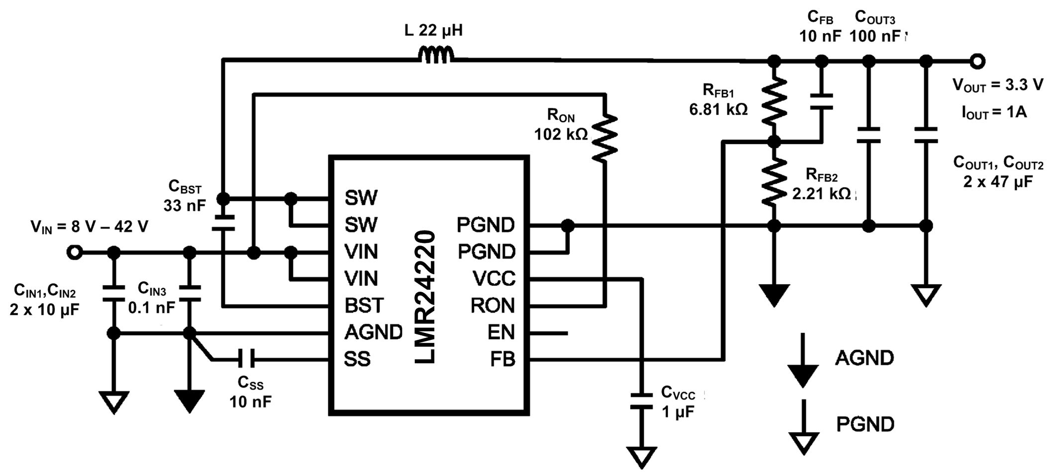
LMR24220 30167635.pngFigure 25. Typical Application Schematic For VOUT = 3.3 V
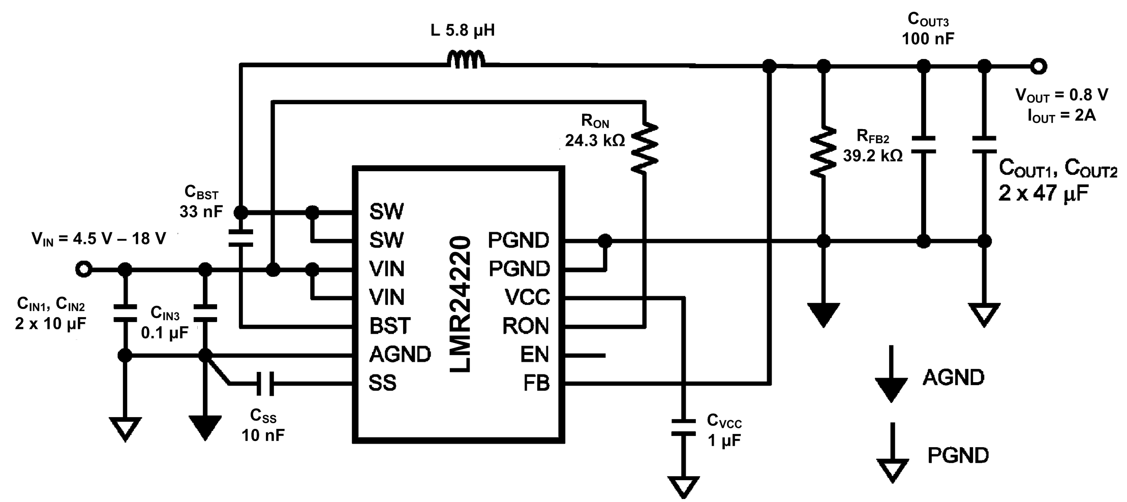
LMR24220 30167636.pngFigure 26. Typical Application Schematic For VOUT = 0.8 V