SNVSC31A march 2023 – may 2023 LMR36501 , LMR36502
PRODUCTION DATA
- 1
- 1 Features
- 2 Applications
- 3 Description
- 4 Revision History
- 5 Device Comparison Table
- 6 Pin Configuration and Functions
- 7 Specifications
-
8 Detailed Description
- 8.1 Overview
- 8.2 Functional Block Diagram
- 8.3
Feature Description
- 8.3.1 Enable, Shutdown, and Start-up
- 8.3.2 Adjustable Switching Frequency (with RT)
- 8.3.3 Power-Good Output Operation
- 8.3.4 Internal LDO, VCC UVLO, and VOUT/FB Input
- 8.3.5 Bootstrap Voltage and VBOOT-UVLO (BOOT Terminal)
- 8.3.6 Output Voltage Selection
- 8.3.7 Soft Start and Recovery from Dropout
- 8.3.8 Current Limit and Short Circuit
- 8.3.9 Thermal Shutdown
- 8.3.10 Input Supply Current
- 8.4 Device Functional Modes
-
9 Application and Implementation
- 9.1 Application Information
- 9.2
Typical Application
- 9.2.1 Design Requirements
- 9.2.2 Detailed Design Procedure
- 9.2.3 Application Curves
- 9.3 Best Design Practices
- 9.4 Power Supply Recommendations
- 9.5 Layout
- 10Device and Documentation Support
- 11Mechanical, Packaging, and Orderable Information
Package Options
Mechanical Data (Package|Pins)
- RPE|9
Thermal pad, mechanical data (Package|Pins)
- RPE|9
Orderable Information
3 Description
The LMR3650x is the industry smallest 65-V, 150-mA, 100-mA synchronous step-down DC/DC converter in 4-mm2 HotRod package. This easy-to-use converter can handle input voltage transients up to 70 V, provide excellent EMI performance and supports fixed, 3.3 V, 5 V and other adjustable output voltages.
The LMR3650x uses the peak current mode control architecture with internal compensation to maintain stable operation with minimal output capacitance. The LMR3650x with the right resistor selection from the RT pin to ground can be externally programmed to any desired switching frequency of operation over a wide range from 200 kHz to 2.2 MHz. The precision EN/UVLO feature allows precise control of the device during the start-up and shutdown. The PGOOD flag, with built-in glitch filter and delayed release, offers a true indication of the system status, eliminating the requirement for an external voltage supervisor. The compact solution size and rich feature set of LMR3650x simplifies implementation for a wide range of industrial applications.
| PART NUMBER | PACKAGE (1) | BODY SIZE (NOM) |
|---|---|---|
| LMR36501 | RPE (VQFN-HR, 9) | 2.00 mm × 2.00 mm |
| LMR36502 | RPE (VQFN-HR, 9) | 2.00 mm × 2.00 mm |
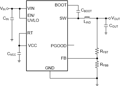
 Simplified Schematic
 Efficiency versus Output Current
 VOUT = 3.3 V (Fixed), 1 MHz, AUTO