SNVSBB5B September 2019 – September 2020 LMR36503-Q1
PRODUCTION DATA
- 1 Features
- 2 Applications
- 3 Description
- 4 Revision History
- 5 Device Comparison Table
- 6 Pin Configuration and Functions
- 7 Specifications
-
8 Detailed Description
- 8.1 Overview
- 8.2 Functional Block Diagram
- 8.3
Feature Description
- 8.3.1 Enable, Start-up and Shutdown
- 8.3.2 External CLK SYNC (with MODE/SYNC)
- 8.3.3 Adjustable Switching Frequency (with RT)
- 8.3.4 Power-Good Output Operation
- 8.3.5 Internal LDO, VCC UVLO, and VOUT/BIAS Input
- 8.3.6 Bootstrap Voltage and VCBOOT-UVLO (CBOOT Terminal)
- 8.3.7 Output Voltage Selection
- 8.3.8 Soft Start and Recovery from Dropout
- 8.3.9 Current Limit and Short Circuit
- 8.3.10 Thermal Shutdown
- 8.3.11 Input Supply Current
- 8.4 Device Functional Modes
-
9 Application and Implementation
- 9.1 Application Information
- 9.2
Typical Application
- 9.2.1 Design Requirements
- 9.2.2 Detailed Design Procedure
- 9.2.3 Application Curves
- 9.3 What to Do and What Not to Do
- 10Power Supply Recommendations
- 11Layout
- 12Device and Documentation Support
- 13Mechanical, Packaging, and Orderable Information
Package Options
Mechanical Data (Package|Pins)
- RPE|9
Thermal pad, mechanical data (Package|Pins)
- RPE|9
Orderable Information
8.3.4 Power-Good Output Operation
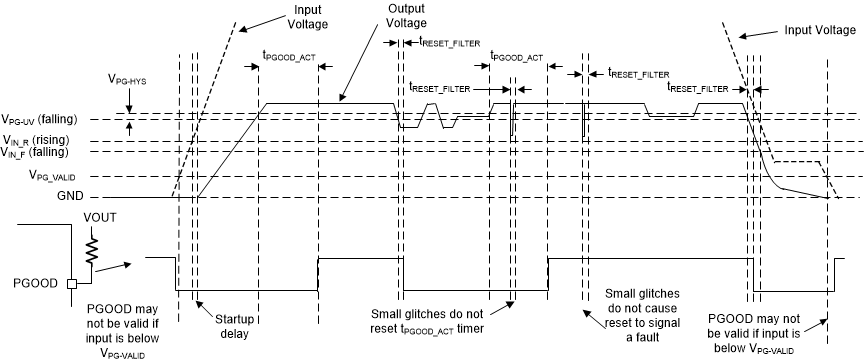
The power-good feature using the PG pin of the LMR36503-Q1 can be used to reset a system microprocessor whenever the output voltage is out of regulation. This open-drain output remains low under device fault conditions, such as current limit and thermal shutdown, as well as during normal start-up. A glitch filter prevents false flag operation for any short duration excursions in the output voltage, such as during line and load transients. Output voltage excursions lasting less than tRESET_FILTER do not trip the power-good flag. Power-good operation can best be understood in reference to Figure 8-8. Table 8-3 gives a more detailed breakdown the PGOOD operation. Here, VPG-UV is defined as the PG-UV scaled version of the VOUT-Reg (target regulated output voltage) and VPG-HYS as the PG-HYS scaled version of the VOUT-Reg, where both PG-UV and PG-HYS are listed in Section 7.5. During the initial power up, a total delay of 5 ms (typ.) is encountered from the time the VEN-VOUT is triggered to the time that the power-good is flagged high. This delay only occurs during the device start-up and is not encountered during any other normal operation of the power-good function. When EN is pulled low, the power-good flag output is also forced low. With EN low, power-good remains valid as long as the input voltage (VPG-VALID is ≥ 1 V (typical).
The power-good output scheme consists of an open-drain n-channel MOSFET, which requires an external pullup resistor connected to a suitable logic supply. It can also be pulled up to either VCC or VOUT through an appropriate resistor, as desired. If this function is not needed, the PGOOD pin can be open or grounded. Limit the current into this pin to ≤ 4 mA.
 Figure 8-8 Power-Good Operation (OV Events Not Included)
| FAULT CONDITION INITIATED | FAULT CONDITION ENDS (AFTER WHICH tPGOOD_ACT MUST PASS BEFORE PGOOD OUTPUT IS RELEASED) |
|---|---|
| VOUT < VPG-UV AND t > tRESET_FILTER | Output voltage in regulation: VPG-UV + VPG-HYS < VOUT < VPG-OV - VPG-HYS |
| VOUT > VPG-OV AND t > tRESET_FILTER | Output voltage in regulation |
| TJ > TSD-R | TJ < TSD-F AND output voltage in regulation |
| EN < VEN-VOUT - VEN-HYST | EN > VEN-VOUT AND output voltage in regulation |
| VCC < VCC-UVLO - VCC-UVLO-HYST | VCC > VCC-UVLO AND output voltage in regulation |