SNVSBB5B September 2019 – September 2020 LMR36503-Q1
PRODUCTION DATA
- 1 Features
- 2 Applications
- 3 Description
- 4 Revision History
- 5 Device Comparison Table
- 6 Pin Configuration and Functions
- 7 Specifications
-
8 Detailed Description
- 8.1 Overview
- 8.2 Functional Block Diagram
- 8.3
Feature Description
- 8.3.1 Enable, Start-up and Shutdown
- 8.3.2 External CLK SYNC (with MODE/SYNC)
- 8.3.3 Adjustable Switching Frequency (with RT)
- 8.3.4 Power-Good Output Operation
- 8.3.5 Internal LDO, VCC UVLO, and VOUT/BIAS Input
- 8.3.6 Bootstrap Voltage and VCBOOT-UVLO (CBOOT Terminal)
- 8.3.7 Output Voltage Selection
- 8.3.8 Soft Start and Recovery from Dropout
- 8.3.9 Current Limit and Short Circuit
- 8.3.10 Thermal Shutdown
- 8.3.11 Input Supply Current
- 8.4 Device Functional Modes
-
9 Application and Implementation
- 9.1 Application Information
- 9.2
Typical Application
- 9.2.1 Design Requirements
- 9.2.2 Detailed Design Procedure
- 9.2.3 Application Curves
- 9.3 What to Do and What Not to Do
- 10Power Supply Recommendations
- 11Layout
- 12Device and Documentation Support
- 13Mechanical, Packaging, and Orderable Information
Package Options
Mechanical Data (Package|Pins)
- RPE|9
Thermal pad, mechanical data (Package|Pins)
- RPE|9
Orderable Information
9.2 Typical Application
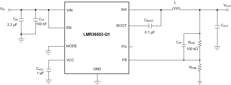
Figure 9-1 shows a typical application circuit for the LMR36503-Q1. This device is designed to function over a wide range of external components and system parameters. However, the internal compensation is optimized for a certain range of external inductance and output capacitance. As a quick-start guide, Table 9-1 provides typical component values for a range of the most common output voltages.
 Figure 9-1 Example Application Circuit
Table 9-1 Typical External Component Values(1)
| ƒSW (kHz) | VOUT (V) | L (µH) | NOMINAL COUT (RATED CAPACITANCE) | MINIMUM COUT (RATED CAPACITANCE) | RFBT (Ω) | RFBB (Ω) | CIN | CBOOT | CVCC |
|---|---|---|---|---|---|---|---|---|---|
| 400 | 3.3 | 68 | 1 x 47 µF | 1 x 22 µF | 100 k | 43.2 k | 2.2 µF + 1 × 100 nF | 100 nF | 1 µF |
| 2200 | 3.3 | 10 | 1 × 10 µF | 1 x 10 µF | 100 k | 43.2 k | 2.2 µF + 1 × 100 nF | 100 nF | 1 µF |
| 400 | 5 | 82 | 1 x 47 µF | 1 × 22 µF | 100 k | 24.9 k | 2.2 µF + 1 × 100 nF | 100 nF | 1 µF |
| 2200 | 5 | 15 | 1 × 10 µF | 1 x 10 µF | 100 k | 24.9 k | 2.2 µF + 1 × 100 nF | 100 nF | 1 µF |
(1) Inductor values
are calculated based on typical VIN = 13.5 V.