SNVSB91C July   2019  – June 2020 LMR36506-Q1

PRODUCTION DATA.  

  1. Features
  2. Applications
  3. Description
    1.     Device Images
      1.      Simplified Schematic
      2.      Efficiency versus Output Current VOUT = 3.3 V (Fixed), 2.2 MHz
  4. Revision History
  5. Device Comparison Table
  6. Pin Configuration and Functions
    1.     Pin Functions
  7. Specifications
    1. 7.1 Absolute Maximum Ratings
    2. 7.2 ESD (Automotive) Ratings
    3. 7.3 Recommended Operating Conditions
    4. 7.4 Thermal Information
    5. 7.5 Electrical Characteristics
    6. 7.6 Timing Characteristics
    7. 7.7 Switching Characteristics
    8. 7.8 System Characteristics
    9. 7.9 Typical Characteristics
  8. Detailed Description
    1. 8.1 Overview
    2. 8.2 Functional Block Diagram
    3. 8.3 Feature Description
      1. 8.3.1  Enable, Start-up and Shutdown
      2. 8.3.2  External CLK SYNC (with MODE/SYNC)
        1. 8.3.2.1 Pulse-Dependent MODE/SYNC Pin Control
      3. 8.3.3  Adjustable Switching Frequency (with RT)
      4. 8.3.4  Power-Good Output Operation
      5. 8.3.5  Internal LDO, VCC UVLO, and VOUT/BIAS Input
      6. 8.3.6  Bootstrap Voltage and VCBOOT-UVLO (CBOOT Terminal)
      7. 8.3.7  Output Voltage Selection
      8. 8.3.8  Spread Spectrum
      9. 8.3.9  Soft Start and Recovery from Dropout
        1. 8.3.9.1 Recovery from Dropout
      10. 8.3.10 Current Limit and Short Circuit
      11. 8.3.11 Thermal Shutdown
      12. 8.3.12 Input Supply Current
    4. 8.4 Device Functional Modes
      1. 8.4.1 Shutdown Mode
      2. 8.4.2 Standby Mode
      3. 8.4.3 Active Mode
        1. 8.4.3.1 CCM Mode
        2. 8.4.3.2 Auto Mode - Light Load Operation
          1. 8.4.3.2.1 Diode Emulation
          2. 8.4.3.2.2 Frequency Reduction
        3. 8.4.3.3 FPWM Mode - Light Load Operation
        4. 8.4.3.4 Minimum On-time (High Input Voltage) Operation
        5. 8.4.3.5 Dropout
  9. Application and Implementation
    1. 9.1 Application Information
    2. 9.2 Typical Application
      1. 9.2.1 Design Requirements
      2. 9.2.2 Detailed Design Procedure
        1. 9.2.2.1 Choosing the Switching Frequency
        2. 9.2.2.2 Setting the Output Voltage
          1. 9.2.2.2.1 FB for Adjustable Output
        3. 9.2.2.3 Inductor Selection
        4. 9.2.2.4 Output Capacitor Selection
        5. 9.2.2.5 Input Capacitor Selection
        6. 9.2.2.6 CBOOT
        7. 9.2.2.7 VCC
        8. 9.2.2.8 CFF Selection
          1. 9.2.2.8.1 External UVLO
        9. 9.2.2.9 Maximum Ambient Temperature
      3. 9.2.3 Application Curves
    3. 9.3 What to Do and What Not to Do
  10. 10Power Supply Recommendations
  11. 11Layout
    1. 11.1 Layout Guidelines
      1. 11.1.1 Ground and Thermal Considerations
    2. 11.2 Layout Example
  12. 12Device and Documentation Support
    1. 12.1 Documentation Support
      1. 12.1.1 Related Documentation
    2. 12.2 Receiving Notification of Documentation Updates
    3. 12.3 Support Resources
    4. 12.4 Trademarks
    5. 12.5 Electrostatic Discharge Caution
    6. 12.6 Glossary
  13. 13Mechanical, Packaging, and Orderable Information

Package Options

Mechanical Data (Package|Pins)
Thermal pad, mechanical data (Package|Pins)
Orderable Information

Device Images

Simplified Schematic

LMR36506-Q1 Simplified_Schematic_MODE.gif

Efficiency versus Output Current
VOUT = 3.3 V (Fixed), 2.2 MHz
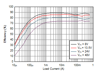
LMR36506-Q1 LMR36506MSC3_Brd1F_Efficiency_2p2MHz_PFM.gif