SNVSB91C July 2019 – June 2020 LMR36506-Q1
PRODUCTION DATA.
- 1 Features
- 2 Applications
- 3 Description
- 4 Revision History
- 5 Device Comparison Table
- 6 Pin Configuration and Functions
- 7 Specifications
-
8 Detailed Description
- 8.1 Overview
- 8.2 Functional Block Diagram
- 8.3
Feature Description
- 8.3.1 Enable, Start-up and Shutdown
- 8.3.2 External CLK SYNC (with MODE/SYNC)
- 8.3.3 Adjustable Switching Frequency (with RT)
- 8.3.4 Power-Good Output Operation
- 8.3.5 Internal LDO, VCC UVLO, and VOUT/BIAS Input
- 8.3.6 Bootstrap Voltage and VCBOOT-UVLO (CBOOT Terminal)
- 8.3.7 Output Voltage Selection
- 8.3.8 Spread Spectrum
- 8.3.9 Soft Start and Recovery from Dropout
- 8.3.10 Current Limit and Short Circuit
- 8.3.11 Thermal Shutdown
- 8.3.12 Input Supply Current
- 8.4 Device Functional Modes
-
9 Application and Implementation
- 9.1 Application Information
- 9.2
Typical Application
- 9.2.1 Design Requirements
- 9.2.2 Detailed Design Procedure
- 9.2.3 Application Curves
- 9.3 What to Do and What Not to Do
- 10Power Supply Recommendations
- 11Layout
- 12Device and Documentation Support
- 13Mechanical, Packaging, and Orderable Information
Package Options
Mechanical Data (Package|Pins)
- RPE|9
Thermal pad, mechanical data (Package|Pins)
- RPE|9
Orderable Information
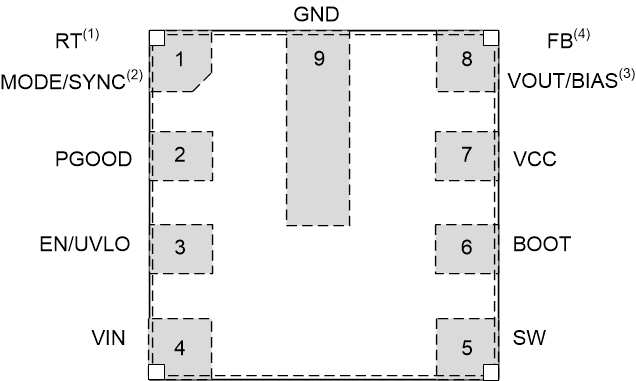
6 Pin Configuration and Functions
RPE Package
9-Pin (2 mm x 2 mm) VQFN-HR
Top View

1. See Device Comparison Table for more details. Pin 1 trimmed and factory-set for externally adjustable switching frequency RT variants only.
2. Pin 1 factory-set for fixed switching frequency MODE/SYNC variants only.
3. Pin 8 trimmed and factory-set for fixed output voltage VOUT/BIAS variants only.
4. Pin 8 factory-set for adjustable output voltage FB variants only.
Pin Functions
| PIN | I/O | DESCRIPTION | ||
|---|---|---|---|---|
| NO. | NAME | |||
| 1 | RT
or MODE/SYNC |
A | When part is trimmed as the RT variant, the switching frequency can be adjusted from 200 kHz to 2.2 MHz.
When the part is trimmed as the MODE/SYNC variant, it can operate in user-selectable PFM/FPWM mode and can be synchronized to an external clock. Do not float this pin. |
|
| 2 | PGOOD | A | Open-drain power-good flag output. Connect to suitable voltage supply through a current limiting resistor. High = power OK, low = power bad. It goes low when EN = low. It can be open or grounded when not used. | |
| 3 | EN/UVLO | A | Enable input to regulator. High = ON, low = OFF. Can be connected directly to VIN. Do not float this pin. | |
| 4 | VIN | P | Input supply to regulator. Connect a high-quality bypass capacitor or capacitors directly to this pin and GND. | |
| 5 | SW | P | Regulator switch node. Connect to power inductor. | |
| 6 | BOOT | P | Bootstrap supply voltage for internal high-side driver. Connect a high-quality 100-nF capacitor from this pin to the SW pin. | |
| 7 | VCC | P | Internal LDO output. Used as supply to internal control circuits. Do not connect to external loads. Can be used as logic supply for power-good flag. Connect a high-quality 1-µF capacitor from this pin to GND. | |
| 8 | VOUT/BIAS or FB | A | Fixed output options are available with the VOUT/BIAS pin variant. Connect to output voltage node for fixed VOUT. Check the Device Comparison Table for more details.
The FB pin variant can help adjust the output voltage. Connect to tap point of feedback voltage divider. Do not float this pin. |
|
| 9 | GND | G | Power ground terminal. Connect to system ground. Connect to CIN with short, wide traces. | |
| A = Analog, P = Power, G = Ground | ||||