SNVSBD7A October   2019  – February 2020 LMR36510

PRODUCTION DATA.  

  1. Features
  2. Applications
  3. Description
    1.     Device Images
      1.      Efficiency versus Output Current VOUT = 5 V, 400 kHz
      2.      Simplified Schematic
  4. Revision History
  5. Pin Configuration and Functions
    1.     Pin Functions
  6. Specifications
    1. 6.1 Absolute Maximum Ratings
    2. 6.2 ESD Ratings
    3. 6.3 Recommended Operating Conditions
    4. 6.4 Thermal Information
    5. 6.5 Electrical Characteristics
    6. 6.6 Timing Requirements
    7. 6.7 Switching Characteristics
    8. 6.8 System Characteristics
    9. 6.9 Typical Characteristics
  7. Detailed Description
    1. 7.1 Overview
    2. 7.2 Functional Block Diagram
    3. 7.3 Feature Description
      1. 7.3.1 Power-Good Flag Output
      2. 7.3.2 Enable and Start-up
      3. 7.3.3 Current Limit and Short Circuit
      4. 7.3.4 Undervoltage Lockout and Thermal Shutdown
    4. 7.4 Device Functional Modes
      1. 7.4.1 Auto Mode
      2. 7.4.2 Dropout
      3. 7.4.3 Minimum Switch On-Time
  8. Application and Implementation
    1. 8.1 Application Information
    2. 8.2 Typical Application
      1. 8.2.1 Design 1: Low Power 24-V, 1-A Buck Converter
        1. 8.2.1.1 Design Requirements
        2. 8.2.1.2 Detailed Design Procedure
          1. 8.2.1.2.1  Choosing the Switching Frequency
          2. 8.2.1.2.2  Setting the Output Voltage
          3. 8.2.1.2.3  Inductor Selection
          4. 8.2.1.2.4  Output Capacitor Selection
          5. 8.2.1.2.5  Input Capacitor Selection
          6. 8.2.1.2.6  CBOOT
          7. 8.2.1.2.7  VCC
          8. 8.2.1.2.8  CFF Selection
          9. 8.2.1.2.9  External UVLO
          10. 8.2.1.2.10 Maximum Ambient Temperature
      2. 8.2.2 Application Curves
    3. 8.3 What to Do and What Not to Do
  9. Power Supply Recommendations
  10. 10Layout
    1. 10.1 Layout Guidelines
      1. 10.1.1 Ground and Thermal Considerations
    2. 10.2 Layout Example
  11. 11Device and Documentation Support
    1. 11.1 Device Support
      1. 11.1.1 Development Support
    2. 11.2 Documentation Support
      1. 11.2.1 Related Documentation
    3. 11.3 Receiving Notification of Documentation Updates
    4. 11.4 Support Resources
    5. 11.5 Trademarks
    6. 11.6 Electrostatic Discharge Caution
    7. 11.7 Glossary
  12. 12Mechanical, Packaging, and Orderable Information

Package Options

Mechanical Data (Package|Pins)
Thermal pad, mechanical data (Package|Pins)
Orderable Information

Enable and Start-up

Start-up and shutdown are controlled by the EN input. This input features precision thresholds, allowing the use of an external voltage divider to provide an adjustable input UVLO (see the External UVLO section). Applying a voltage of ≥ VEN-VCC_H causes the device to enter standby mode, powering the internal VCC, but not producing an output voltage. Increasing the EN voltage to VEN-H fully enables the device, allowing it to enter start-up mode and begin the soft-start period. When the EN input is brought below VEN-H by VEN-HYS, the regulator stops running and enters standby mode. If the EN voltage decreases below VEN-VCC-L, the device shuts down. Figure 5 shows this behavior. The EN input can be connected directly to VIN if this feature is not needed. This input must not be allowed to float. The values for the various EN thresholds can be found in the Electrical Characteristics table.

The LMR36510 utilizes a reference-based soft start that prevents output voltage overshoots and large inrush currents as the regulator is starting up.
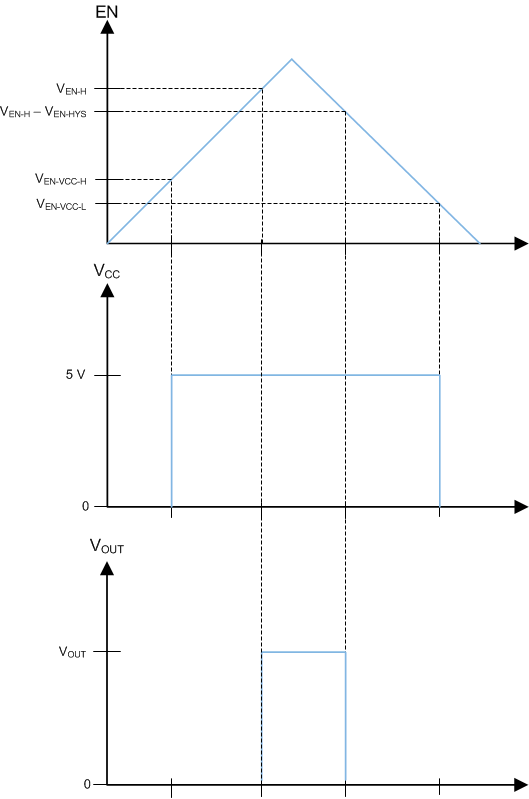
LMR36510 LMR360XX-EN-threshold-plot-snvsay7.gifFigure 5. Precision Enable Behavior
LMR36510 EN_Startup_Waveform.gifFigure 6. Typical Start-up Behavior
VIN = 24 V, VOUT = 5 V, IOUT = 1 A