SNVSCJ0A November   2023  – February 2024 LMR38025-Q1

PRODUCTION DATA  

  1.   1
  2. Features
  3. Applications
  4. Description
  5. Device Comparison Table
  6. Pin Configuration and Functions
  7. Specifications
    1. 6.1 Absolute Maximum Ratings
    2. 6.2 ESD Ratings
    3. 6.3 Recommended Operating Conditions
    4. 6.4 Thermal Information
    5. 6.5 Electrical Characteristics
    6. 6.6 System Characteristics
    7. 6.7 Typical Characteristics
  8. Detailed Description
    1. 7.1 Overview
    2. 7.2 Functional Block Diagram
    3. 7.3 Feature Description
      1. 7.3.1  Fixed Frequency Peak Current Mode Control
      2. 7.3.2  Adjustable Output Voltage
      3. 7.3.3  Enable
      4. 7.3.4  Switching Frequency and Synchronization (RT/SYNC)
      5. 7.3.5  Power-Good Flag Output
      6. 7.3.6  Minimum On Time, Minimum Off Time, and Frequency Foldback
      7. 7.3.7  Bootstrap Voltage
      8. 7.3.8  Overcurrent and Short-Circuit Protection
      9. 7.3.9  Soft Start
      10. 7.3.10 Thermal Shutdown
    4. 7.4 Device Functional Modes
      1. 7.4.1 Auto Mode
      2. 7.4.2 Forced PWM Operation
      3. 7.4.3 Dropout
      4. 7.4.4 Minimum Switch On Time
  9. Application and Implementation
    1. 8.1 Application Information
    2. 8.2 Typical Application
      1. 8.2.1 Design Requirements
      2. 8.2.2 Detailed Design Procedure
        1. 8.2.2.1 Custom Design With WEBENCH® Tools
        2. 8.2.2.2 Choosing the Switching Frequency
        3. 8.2.2.3 FB for Adjustable Output
        4. 8.2.2.4 Inductor Selection
        5. 8.2.2.5 Output Capacitor Selection
        6. 8.2.2.6 Input Capacitor Selection
        7. 8.2.2.7 CBOOT
        8. 8.2.2.8 External UVLO
        9. 8.2.2.9 Maximum Ambient Temperature
      3. 8.2.3 Application Curves
    3. 8.3 Best Design Practices
    4. 8.4 Power Supply Recommendations
    5. 8.5 Layout
      1. 8.5.1 Layout Guidelines
        1. 8.5.1.1 Ground and Thermal Considerations
      2. 8.5.2 Layout Example
  10. Device and Documentation Support
    1. 9.1 Device Support
      1. 9.1.1 Third-Party Products Disclaimer
      2. 9.1.2 Development Support
        1. 9.1.2.1 Custom Design With WEBENCH® Tools
    2. 9.2 Documentation Support
      1. 9.2.1 Related Documentation
    3. 9.3 Receiving Notification of Documentation Updates
    4. 9.4 Support Resources
    5. 9.5 Trademarks
    6. 9.6 Electrostatic Discharge Caution
    7. 9.7 Glossary
  11. 10Revision History
  12. 11Mechanical, Packaging, and Orderable Information

Package Options

Mechanical Data (Package|Pins)
Thermal pad, mechanical data (Package|Pins)
Orderable Information

Typical Characteristics

Unless otherwise specified the following conditions apply: TA = 25°C, VIN = 24V, fSW = 400kHz
GUID-20240129-SS0I-KK9C-GRTR-7LDCHPLWHPH6-low.png
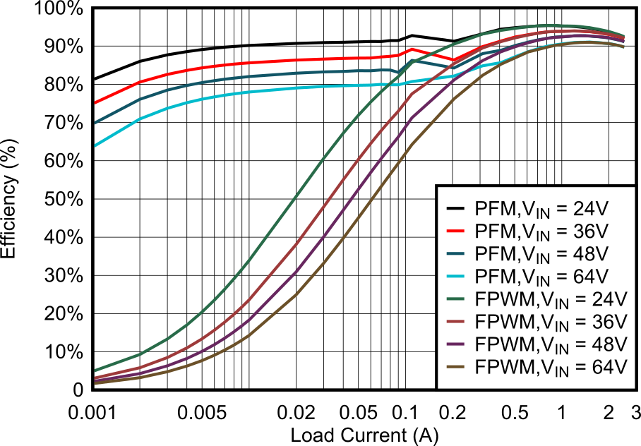
FSW = 400kHz VOUT = 12.0V
Figure 6-1 Efficiency vs Load Current
GUID-20240201-SS0I-FPM3-QZ7D-HWTKJZMTJTVZ-low.svg
FSW = 400kHz VOUT = 5.0V PFM version
Figure 6-3 5V Dropout
GUID-20231031-SS0I-893M-6LC5-8XWMNM7S75WN-low.svgFigure 6-5 High-Side and Low-Side Current Limit vs Temperature
GUID-20230929-SS0I-NQVZ-B5WK-C59MBDCGGVTG-low.svg
VOUT = 5V RFBB = 100k
Figure 6-2 No Load Input Current vs Input Voltage
GUID-20231031-SS0I-16GX-KHDM-6XPFKMHQ1FVT-low.svg
VIN = 48.0V
Figure 6-4 Reference Voltage vs Temperature
GUID-20231031-SS0I-SGVR-N4HV-MQ3VVPK8WKVW-low.svgFigure 6-6 VIN UVLO vs Temperature