SNVSCJ0A November 2023 – February 2024 LMR38025-Q1
PRODUCTION DATA
- 1
- 1 Features
- 2 Applications
- 3 Description
- 4 Device Comparison Table
- 5 Pin Configuration and Functions
- 6 Specifications
-
7 Detailed Description
- 7.1 Overview
- 7.2 Functional Block Diagram
- 7.3
Feature Description
- 7.3.1 Fixed Frequency Peak Current Mode Control
- 7.3.2 Adjustable Output Voltage
- 7.3.3 Enable
- 7.3.4 Switching Frequency and Synchronization (RT/SYNC)
- 7.3.5 Power-Good Flag Output
- 7.3.6 Minimum On Time, Minimum Off Time, and Frequency Foldback
- 7.3.7 Bootstrap Voltage
- 7.3.8 Overcurrent and Short-Circuit Protection
- 7.3.9 Soft Start
- 7.3.10 Thermal Shutdown
- 7.4 Device Functional Modes
- 8 Application and Implementation
- 9 Device and Documentation Support
- 10Revision History
- 11Mechanical, Packaging, and Orderable Information
Package Options
Mechanical Data (Package|Pins)
- DRR|12
Thermal pad, mechanical data (Package|Pins)
- DRR|12
Orderable Information
3 Description
The LMR38025-Q1 synchronous buck converter is designed to regulate over a wide input voltage range, minimizing the need for external surge suppression components. The LMR38025-Q1 operates during input voltage dips as low as 4.2V, at nearly 100% duty cycle if needed, making the device an excellent choice for 48V battery automotive applications and MHEV/EV systems as the absolute maximum input voltage is 85V.
The LMR38025-Q1 features a high voltage enable pin to enable the device by connecting the device to the wide input supply voltage or by having precise UVLO control across start-up and shutdown. The power-good flag, with built-in filtering and delay, offers a true indication of system status, eliminating the need for an external supervisor. The device incorporates pseudorandom spread spectrum option for minimal EMI. The switching frequency can be configured between 200kHz and 2.2MHz to avoid noise sensitive frequency bands. In addition, the frequency can be programmed through the RT pin for improved efficiency at low operating frequencies or by having a smaller design size at high operating frequencies.
The device has built-in protection features such as cycle-by-cycle current limit, hiccup mode short-circuit protection, and thermal shutdown in case of excessive power dissipation. The LMR38025-Q1 is qualified to automotive AEC-Q100 grade 1 and is available in a 12-pin WSON package.
| PART NUMBER | PACKAGE(1) | PACKAGE SIZE(2) |
|---|---|---|
| LMR38025-Q1 | DRR (WSON, 12) | 3.00mm × 3.00mm |
 Simplified Schematic
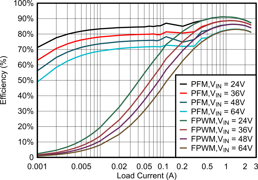
 Efficiency vs Output Current VOUT = 5V, 400kHz