SLUSDW3A April   2020  – November 2020 LMR50410

PRODUCTION DATA  

  1. Features
  2. Applications
  3. Description
  4. Revision History
  5. Device Comparison Table
  6. Pin Configuration and Functions
  7. Specifications
    1. 7.1 Absolute Maximum Ratings
    2. 7.2 ESD Ratings
    3. 7.3 Recommended Operating Conditions
    4. 7.4 Thermal Information
    5. 7.5 Electrical Characteristics
    6. 7.6 Timing Requirements
    7. 7.7 Switching Characteristics
    8. 7.8 System Characteristics
    9. 7.9 Typical Characteristics
  8. Detailed Description
    1. 8.1 Overview
    2. 8.2 Functional Block Diagram
    3. 8.3 Feature Description
      1. 8.3.1 Fixed Frequency Peak Current Mode Control
      2. 8.3.2 Adjustable Output Voltage
      3. 8.3.3 Enable
      4. 8.3.4 Minimum ON-Time, Minimum OFF-Time, and Frequency Foldback
      5. 8.3.5 Bootstrap Voltage
      6. 8.3.6 Overcurrent and Short Circuit Protection
      7. 8.3.7 Soft Start
      8. 8.3.8 Thermal Shutdown
    4. 8.4 Device Functional Modes
      1. 8.4.1 Shutdown Mode
      2. 8.4.2 Active Mode
      3. 8.4.3 CCM Mode
      4. 8.4.4 Light-Load Operation (PFM Version)
      5. 8.4.5 Light-Load Operation (FPWM Version)
  9. Application and Implementation
    1. 9.1 Application Information
    2. 9.2 Typical Application
      1. 9.2.1 Design Requirements
      2. 9.2.2 Detailed Design Procedure
        1. 9.2.2.1 Custom Design With WEBENCH® Tools
        2. 9.2.2.2 Output Voltage Set-Point
        3. 9.2.2.3 Switching Frequency
        4. 9.2.2.4 Inductor Selection
        5. 9.2.2.5 Output Capacitor Selection
        6. 9.2.2.6 Input Capacitor Selection
        7. 9.2.2.7 Bootstrap Capacitor
        8. 9.2.2.8 Undervoltage Lockout Set-Point
      3. 9.2.3 Application Curves
  10. 10Power Supply Recommendations
  11. 11Layout
    1. 11.1 Layout Guidelines
      1. 11.1.1 Compact Layout for EMI Reduction
      2. 11.1.2 Feedback Resistors
    2. 11.2 Layout Example
  12. 12Device and Documentation Support
    1. 12.1 Device Support
      1. 12.1.1 Development Support
        1. 12.1.1.1 Custom Design With WEBENCH® Tools
    2. 12.2 Documentation Support
      1. 12.2.1 Related Documentation
    3. 12.3 Receiving Notification of Documentation Updates
    4. 12.4 Support Resources
    5. 12.5 Trademarks
    6. 12.6 Electrostatic Discharge Caution
    7. 12.7 Glossary
  13. 13Mechanical, Packaging, and Orderable Information

Package Options

Mechanical Data (Package|Pins)
Thermal pad, mechanical data (Package|Pins)
Orderable Information

Typical Characteristics

VIN = 12 V, fSW = 700 kHz ,TA = 25°C, unless otherwise specified.
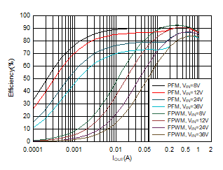
GUID-20201027-CA0I-DPWF-QXFK-HGLPGRCPR0KT-low.gif
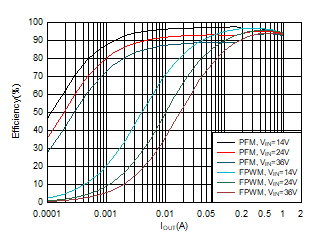
fSW = 700 kHz VOUT = 3.3 V
Figure 7-1 3.3-V Efficiency versus Load Current
GUID-20201027-CA0I-TTNR-BP0D-CF9B6ZNZFHQ6-low.gif
fSW = 700 kHz VOUT = 12 V
Figure 7-3 12-V Efficiency versus Load Current
GUID-25E53BBE-C124-4D80-B344-E170CF5B2F3B-low.gif
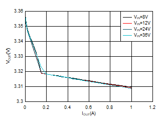
fSW = 700 kHz VOUT = 3.3 V PFM version
Figure 7-5 3.3-V Load Regulation
GUID-78148AEE-51B7-45FB-85F7-EB0F58725E8D-low.gif
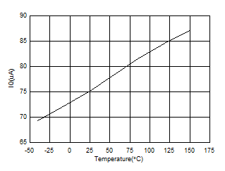
Figure 7-7 IQ versus Temperature
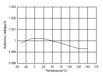
GUID-E81FD66B-DBD0-4D6B-80FA-B17F2868E53B-low.gifFigure 7-9 Reference Voltage versus Temperature
GUID-20201027-CA0I-QVQJ-BPMR-NMXXVPZ8VT3Q-low.gif
fSW = 700 kHz VOUT = 5 V
Figure 7-2 5-V Efficiency versus Load Current
GUID-D00FCFD5-38C7-4D4B-8F34-B75CC2B86759-low.gif
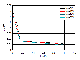
fSW = 700 kHz VOUT = 5 V PFM version
Figure 7-4 5-V Load Regulation
GUID-06765265-B581-4D4E-B084-9BDB68E724A5-low.gif
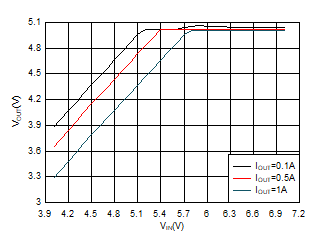
fSW = 700 kHz VOUT = 5 V FPM version
Figure 7-6 5-V Dropout
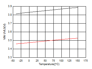
GUID-777A541E-AE2C-464B-9639-B6C4F86334C1-low.gif
Figure 7-8 VIN UVLO versus Temperature
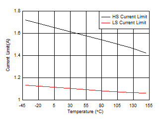
GUID-20200721-CA0I-1DMD-J4VR-VLWCFWWNCVFQ-low.gifFigure 7-10 HS and LS Current Limit versus Temperature