SLUSFV7 November 2024 LMR51403
PRODUCTION DATA
- 1
- 1 Features
- 2 Applications
- 3 Description
- 4 Device Comparison Table
- 5 Pin Configuration and Functions
- 6 Specifications
- 7 Detailed Description
-
8 Application and Implementation
- 8.1 Application Information
- 8.2
Typical Application
- 8.2.1 Design Requirements
- 8.2.2
Detailed Design Procedure
- 8.2.2.1 Custom Design With WEBENCH® Tools
- 8.2.2.2 Output Voltage Setpoint
- 8.2.2.3 Switching Frequency
- 8.2.2.4 Inductor Selection
- 8.2.2.5 Output Capacitor Selection
- 8.2.2.6 Input Capacitor Selection
- 8.2.2.7 Bootstrap Capacitor
- 8.2.2.8 Undervoltage Lockout Setpoint
- 8.2.2.9 Replacing Non Sync Buck Converter
- 8.2.3 Application Curves
- 8.3 Power Supply Recommendations
- 8.4 Layout
- 9 Device and Documentation Support
- 10Revision History
- 11Mechanical, Packaging, and Orderable Information
Package Options
Mechanical Data (Package|Pins)
- DBV|6
Thermal pad, mechanical data (Package|Pins)
Orderable Information
7.3.2 Adjustable Output Voltage
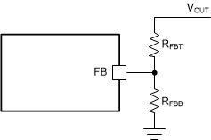
A precision 0.8V reference voltage (VREF) is used to maintain a tightly regulated output voltage over the entire operating temperature range. The output voltage is set by a resistor divider from VOUT to the FB pin. TI recommends to use 1% tolerance resistors with a low temperature coefficient for the FB divider. Select the bottom-side resistor, RFBB, for the desired divider current and use Equation 1 to calculate the top-side resistor, RFBT. The recommended range for RFBT is 10kΩ to 100kΩ. A lower RFBT value can be used if pre-loading is desired to reduce the VOUT offset in PFM operation. Lower RFBT values reduce efficiency at very light load. Less static current goes through a larger RFBT value and can be more desirable when light-load efficiency is critical. However, TI does not recommend RFBT values larger than 1MΩ make the feedback path more susceptible to noise. Larger RFBT values require a more carefully designed feedback path trace from the feedback resistors to the feedback pin of the device. The tolerance and temperature variation of the resistor divider network affect the output voltage regulation.
 Figure 7-2 Output Voltage Setting