SLUSFM3 September 2024 LMR51425-Q1 , LMR51435-Q1
PRODUCTION DATA
- 1
- 1 Features
- 2 Applications
- 3 Description
- 4 Device Comparison Table
- 5 Pin Configuration and Functions
- 6 Specifications
-
7 Detailed Description
- 7.1 Overview
- 7.2 Functional Block Diagram
- 7.3
Feature Description
- 7.3.1 Fixed Frequency Peak Current Mode Control
- 7.3.2 Adjustable Output Voltage
- 7.3.3 Enable
- 7.3.4 Switching Frequency
- 7.3.5 Power-Good Flag Output
- 7.3.6 Minimum ON-Time, Minimum OFF-Time, and Frequency Foldback
- 7.3.7 Bootstrap Voltage
- 7.3.8 Overcurrent and Short-Circuit Protection
- 7.3.9 Soft Start
- 7.3.10 Thermal Shutdown
- 7.4 Device Functional Modes
- 8 Application and Implementation
- 9 Device and Documentation Support
- 10Revision History
- 11Mechanical, Packaging, and Orderable Information
Package Options
Mechanical Data (Package|Pins)
- DRR|12
Thermal pad, mechanical data (Package|Pins)
- DRR|12
Orderable Information
3 Description
The LMR514x5-Q1 is a wide-VIN, easy-to-use, synchronous buck converter capable of driving up to 2.5A or 3.5A load current. With a wide input range of 4V to 36V, the device is designed for a wide range of industrial applications for power conditioning from an unregulated source.
The LMR514x5-Q1 features adjustable switching frequency from 200kHz to 1MHz with an external resistor, which provides the flexibility to optimize either efficiency or external component size. The device has pulse frequency modulation (PFM version) to realize high efficiency at light load, and forced pulse width modulation (FPWM version) to achieve constant frequency, and small output voltage ripple over the full load range. Soft-start and compensation circuits are implemented internally, which allows the device to be used with minimum external components.
The device has built-in protection features, such as cycle-by-cycle current limit, hiccup mode short-circuit protection, and thermal shutdown in case of excessive power dissipation. The LMR514x5-Q1 is available in a WSON-12 package.
| PART NUMBER(1) | CURRENT | PACKAGE(2) | BODY SIZE (NOM) |
|---|---|---|---|
| LMR51425-Q1 | 2.5A | DRR (WSON, 12) | 3.00mm × 3.00mm |
| LMR51435-Q1 | 3.5A |
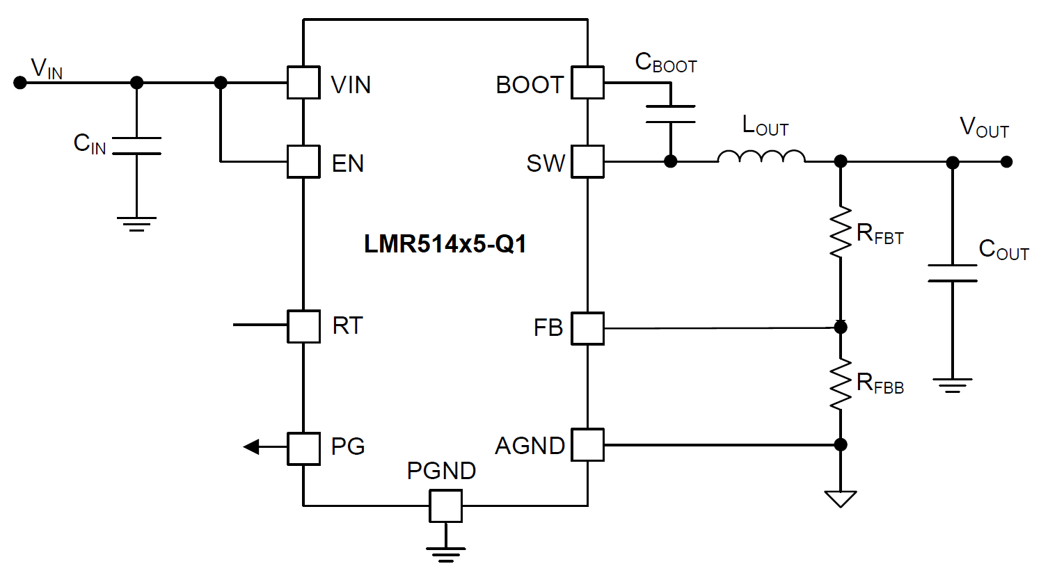
 Simplified Schematic
 Efficiency vs Output Current VOUT = 5V, 440kHz