SLUSFM3 September 2024 LMR51425-Q1 , LMR51435-Q1
PRODUCTION DATA
- 1
- 1 Features
- 2 Applications
- 3 Description
- 4 Device Comparison Table
- 5 Pin Configuration and Functions
- 6 Specifications
-
7 Detailed Description
- 7.1 Overview
- 7.2 Functional Block Diagram
- 7.3
Feature Description
- 7.3.1 Fixed Frequency Peak Current Mode Control
- 7.3.2 Adjustable Output Voltage
- 7.3.3 Enable
- 7.3.4 Switching Frequency
- 7.3.5 Power-Good Flag Output
- 7.3.6 Minimum ON-Time, Minimum OFF-Time, and Frequency Foldback
- 7.3.7 Bootstrap Voltage
- 7.3.8 Overcurrent and Short-Circuit Protection
- 7.3.9 Soft Start
- 7.3.10 Thermal Shutdown
- 7.4 Device Functional Modes
- 8 Application and Implementation
- 9 Device and Documentation Support
- 10Revision History
- 11Mechanical, Packaging, and Orderable Information
Package Options
Mechanical Data (Package|Pins)
- DRR|12
Thermal pad, mechanical data (Package|Pins)
- DRR|12
Orderable Information
11.1 Tape and Reel Information
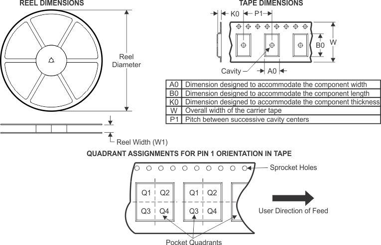
| Device | Package Type |
Package Drawing | Pins | SPQ | Reel Diameter (mm) |
Reel Width W1 (mm) |
A0 (mm) |
B0 (mm) |
K0 (mm) |
P1 (mm) |
W (mm) |
Pin1 Quadrant |
|---|---|---|---|---|---|---|---|---|---|---|---|---|
| LMR51435SQDRRRQ1 | WSON | DRR | 12 | 3000 | 330.0 | 12.4 | 3.3 | 3.3 | 1.1 | 8.0 | 12.0 | Q2 |
| LMR51435FSQDRRRQ1 | WSON | DRR | 12 | 3000 | 330.0 | 12.4 | 3.3 | 3.3 | 1.1 | 8.0 | 12.0 | Q2 |
| LMR51425SQDRRRQ1 | WSON | DRR | 12 | 3000 | 330.0 | 12.4 | 3.3 | 3.3 | 1.1 | 8.0 | 12.0 | Q2 |
| LMR51425FSQDRRRQ1 | WSON | DRR | 12 | 3000 | 330.0 | 12.4 | 3.3 | 3.3 | 1.1 | 8.0 | 12.0 | Q2 |
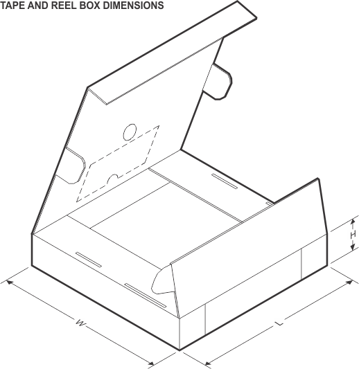
| Device | Package Type | Package Drawing | Pins | SPQ | Length (mm) | Width (mm) | Height (mm) |
|---|---|---|---|---|---|---|---|
| LMR51435SQDRRRQ1 | WSON | DRR | 12 | 3000 | 367.0 | 367.0 | 35.0 |
| LMR51435FSQDRRRQ1 | WSON | DRR | 12 | 3000 | 367.0 | 367.0 | 35.0 |
| LMR51425SQDRRRQ1 | WSON | DRR | 12 | 3000 | 367.0 | 367.0 | 35.0 |
| LMR51425FSQDRRRQ1 | WSON | DRR | 12 | 3000 | 367.0 | 367.0 | 35.0 |