SLUSEP7 December 2022 LMR51440 , LMR51450
PRODUCTION DATA
- 1 Features
- 2 Applications
- 3 Description
- 4 Revision History
- 5 Device Comparison Table
- 6 Pin Configuration and Functions
- 7 Specifications
-
8 Detailed Description
- 8.1 Overview
- 8.2 Functional Block Diagram
- 8.3
Feature Description
- 8.3.1 Fixed Frequency Peak Current Mode Control
- 8.3.2 Adjustable Output Voltage
- 8.3.3 Enable
- 8.3.4 Switching Frequency
- 8.3.5 Power-Good Flag Output
- 8.3.6 Minimum ON-Time, Minimum OFF-Time, and Frequency Foldback
- 8.3.7 Bootstrap Voltage
- 8.3.8 Overcurrent and Short-Circuit Protection
- 8.3.9 Soft Start
- 8.3.10 Thermal Shutdown
- 8.4 Device Functional Modes
- 9 Application and Implementation
- 10Device and Documentation Support
- 11Mechanical, Packaging, and Orderable Information
Package Options
Mechanical Data (Package|Pins)
- DRR|12
Thermal pad, mechanical data (Package|Pins)
- DRR|12
Orderable Information
8.3.5 Power-Good Flag Output
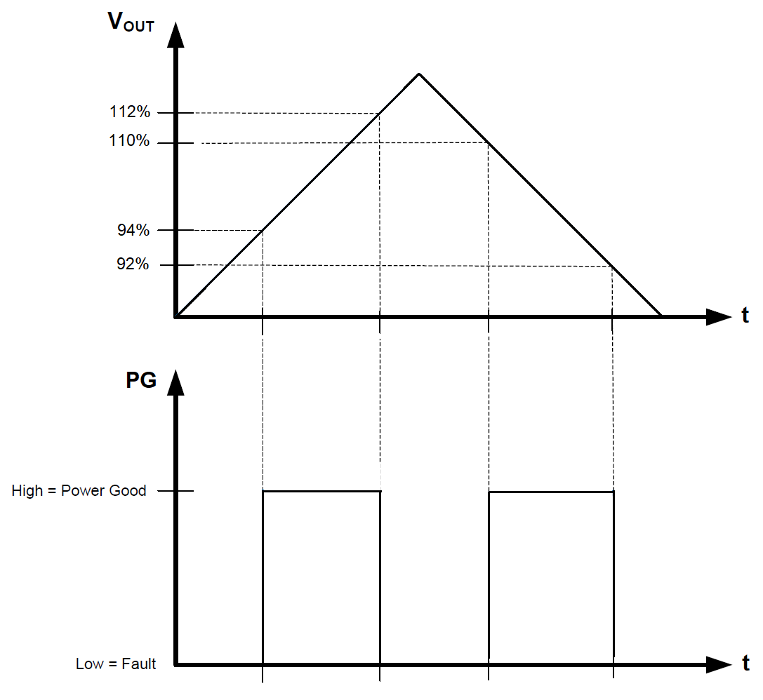
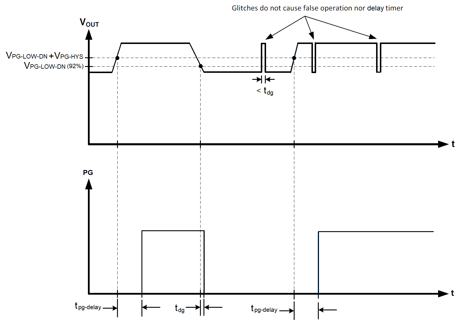
The power-good flag function (PG output pin) of the LMR514x0 can be used to reset a system microprocessor whenever the output voltage is out of regulation. This open-drain output goes low under fault conditions, such as current limit and thermal shutdown, as well as during normal start-up. A glitch filter prevents false flag operation for short excursions of the output voltage, such as during line and load transients. Output voltage excursions lasting less than tdg 35 μs (typical) do not trip the power-good flag. After the FB voltage has returned to the regulation value and after a delay of tpg-delay 3.1 ms (typical) , the power-good flag goes high.
The power-good output consists of an open-drain NMOS, requiring an external pullup resistor to a suitable logic supply. It can be pulled up to power supply below 20 V through a 10-kΩ to 100-kΩ resistor, as desired. If this function is not needed, the PG pin must be left floating. When EN is pulled low, the flag output is also forced low. With EN low, power good remains valid as long as the input voltage is greater than or equal to 1.5 V (typical). Limit the current into the power-good flag pin to less than 5-mA D.C.
 Figure 8-5 Static Power-Good Operation
 Figure 8-6 Power-Good Timing Behavior (OV Events Not Included)