SLUSFR3 August   2024 LMR51460-Q1

PRODUCTION DATA  

  1.   1
  2. Features
  3. Applications
  4. Description
  5. Device Comparison Table
  6. Pin Configuration and Functions
  7. Specifications
    1. 6.1 Absolute Maximum Ratings
    2. 6.2 ESD Ratings
    3. 6.3 Recommended Operating Conditions
    4. 6.4 Thermal Information
    5. 6.5 Electrical Characteristics
    6. 6.6 System Characteristics
    7. 6.7 Typical Characteristics
  8. Detailed Description
    1. 7.1 Overview
    2. 7.2 Functional Block Diagram
    3. 7.3 Feature Description
      1. 7.3.1  Fixed Frequency Peak Current Mode Control
      2. 7.3.2  Adjustable Output Voltage
      3. 7.3.3  Enable
      4. 7.3.4  Switching Frequency
      5. 7.3.5  Power-Good Flag Output
      6. 7.3.6  Minimum ON-Time, Minimum OFF-Time, and Frequency Foldback
      7. 7.3.7  Bootstrap Voltage
      8. 7.3.8  Overcurrent and Short-Circuit Protection
      9. 7.3.9  Soft Start
      10. 7.3.10 Thermal Shutdown
    4. 7.4 Device Functional Modes
      1. 7.4.1 Shutdown Mode
      2. 7.4.2 Active Mode
      3. 7.4.3 CCM Mode
      4. 7.4.4 Light-Load Operation (PFM Version)
      5. 7.4.5 Light-Load Operation (FPWM Version)
  9. Application and Implementation
    1. 8.1 Application Information
    2. 8.2 Typical Application
      1. 8.2.1 Design Requirements
      2. 8.2.2 Detailed Design Procedure
        1. 8.2.2.1 Custom Design With WEBENCH® Tools
        2. 8.2.2.2 Output Voltage Set-Point
        3. 8.2.2.3 Switching Frequency
        4. 8.2.2.4 Inductor Selection
        5. 8.2.2.5 Output Capacitor Selection
        6. 8.2.2.6 Input Capacitor Selection
        7. 8.2.2.7 Bootstrap Capacitor
        8. 8.2.2.8 Undervoltage Lockout Setpoint
      3. 8.2.3 Application Curves
    3. 8.3 Power Supply Recommendations
    4. 8.4 Layout
      1. 8.4.1 Layout Guidelines
        1. 8.4.1.1 Compact Layout for EMI Reduction
        2. 8.4.1.2 Feedback Resistors
      2. 8.4.2 Layout Example
  10. Device and Documentation Support
    1. 9.1 Device Support
      1. 9.1.1 Development Support
        1. 9.1.1.1 Custom Design With WEBENCH® Tools
    2. 9.2 Documentation Support
      1. 9.2.1 Related Documentation
    3. 9.3 Receiving Notification of Documentation Updates
    4. 9.4 Support Resources
    5. 9.5 Trademarks
    6. 9.6 Electrostatic Discharge Caution
    7. 9.7 Glossary
  11. 10Revision History
  12. 11Mechanical, Packaging, and Orderable Information
    1. 11.1 Tape and Reel Information

Package Options

Mechanical Data (Package|Pins)
Thermal pad, mechanical data (Package|Pins)
Orderable Information

Switching Frequency

The switching frequency of the LMR51460-Q1 can be programmed by the resistor RT from the RT pin and GND pin. The RT pin cannot be left floating or shorted to ground. To determine the timing resistance for a given switching frequency, use Equation 2 or the curve in Figure 7-4. Table 7-1 gives typical RT values for a given fSW.

Equation 2. R T k Ω = 18576 ×   f S W k H z   - 1.048
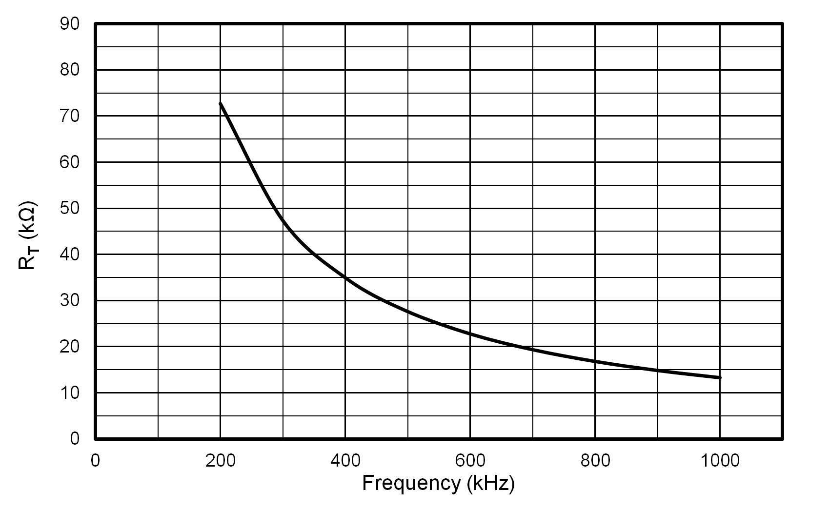
LMR51460-Q1 RT Versus Frequency CurveFigure 7-4 RT Versus Frequency Curve
Table 7-1 Typical Frequency Setting RT Resistance
fSW (kHz)RT (kΩ)
20071.5
400

34.8

440

Open or pull up to voltage >1.0 V

500

27.4

750

18.0

1000

13.3

1000

Short to GND