SLUSFS7 September 2024 LMR51603-Q1
PRODUCTION DATA
- 1
- 1 Features
- 2 Applications
- 3 Description
- 4 Device Comparison Table
- 5 Pin Configuration and Functions
- 6 Specifications
- 7 Detailed Description
-
8 Application and Implementation
- 8.1 Application Information
- 8.2
Typical Application
- 8.2.1 Design Requirements
- 8.2.2
Detailed Design Procedure
- 8.2.2.1 Custom Design With WEBENCH® Tools
- 8.2.2.2 Output Voltage Setpoint
- 8.2.2.3 Switching Frequency
- 8.2.2.4 Inductor Selection
- 8.2.2.5 Output Capacitor Selection
- 8.2.2.6 Input Capacitor Selection
- 8.2.2.7 Bootstrap Capacitor
- 8.2.2.8 Undervoltage Lockout Setpoint
- 8.2.2.9 Replacing Non Sync Buck Converter
- 8.2.3 Application Curves
- 8.3 Power Supply Recommendations
- 8.4 Layout
- 9 Device and Documentation Support
- 10Revision History
- 11Mechanical, Packaging, and Orderable Information
Package Options
Mechanical Data (Package|Pins)
- DBV|6
Thermal pad, mechanical data (Package|Pins)
Orderable Information
3 Description
The LMR51603-Q1 is a wide-VIN, easy-to-use, synchronous buck converter capable of driving up to 300mA load current. With a wide input range of 4V to 65V, the device is designed for a wide range of industrial applications for power conditioning from an unregulated source.
The LMR51603-Q1 operates at 400kHz switching frequency to support use of relatively small inductors for an optimized design size. The LMR51603-Q1 has a pulse frequency modulation (PFM version) to realize high efficiency at light load and forced pulse width modulation (FPWM version) to achieve constant frequency and small output voltage ripple over the full load range. Soft-start and compensation circuits are implemented internally, which allow the device to be used with minimal external components.
The device has built-in protection features, such as cycle-by-cycle current limit, hiccup mode short-circuit protection, and thermal shutdown in case of excessive power dissipation.
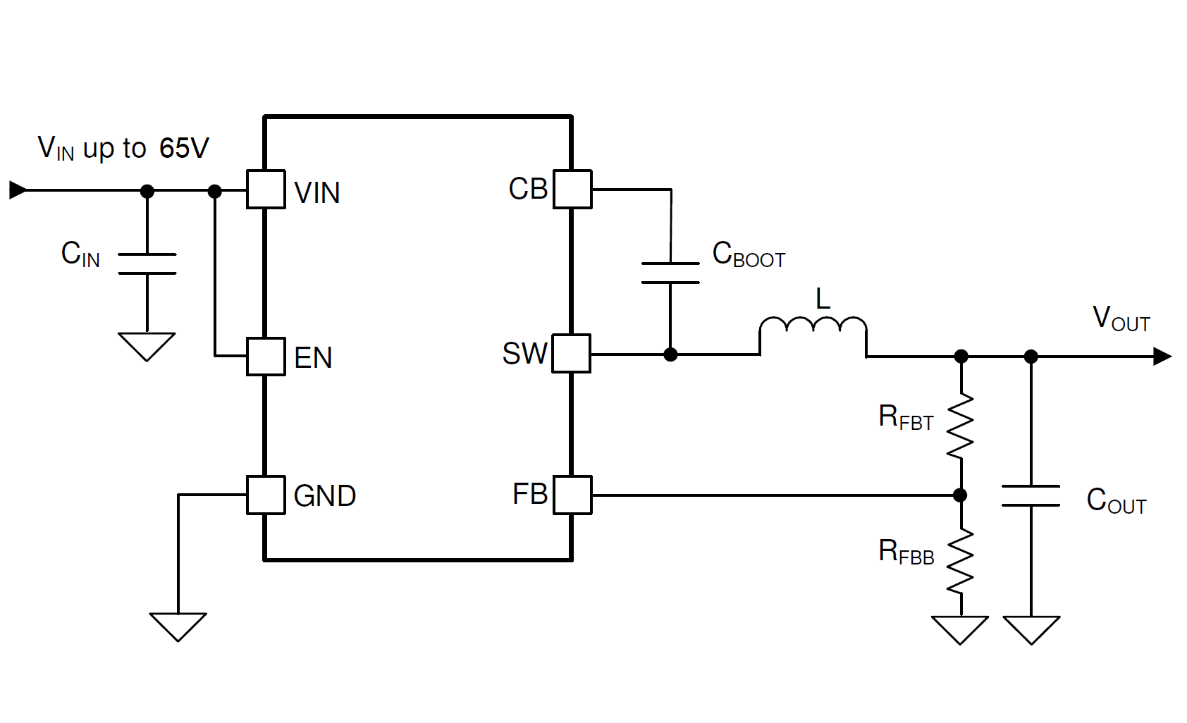
 Simplified Schematic
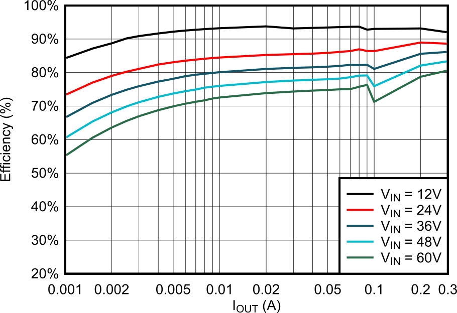
 Efficiency Versus Output Current
 VOUT = 5V, 400kHz