SLUSFO3 November 2024 LMR51603
PRODUCTION DATA
- 1
- 1 Features
- 2 Applications
- 3 Description
- 4 Device Comparison Table
- 5 Pin Configuration and Functions
- 6 Specifications
- 7 Detailed Description
-
8 Application and Implementation
- 8.1 Application Information
- 8.2
Typical Application
- 8.2.1 Design Requirements
- 8.2.2
Detailed Design Procedure
- 8.2.2.1 Custom Design With WEBENCH® Tools
- 8.2.2.2 Output Voltage Setpoint
- 8.2.2.3 Switching Frequency
- 8.2.2.4 Inductor Selection
- 8.2.2.5 Output Capacitor Selection
- 8.2.2.6 Input Capacitor Selection
- 8.2.2.7 Bootstrap Capacitor
- 8.2.2.8 Undervoltage Lockout Setpoint
- 8.2.2.9 Replacing Non-Sync Buck Converter
- 8.2.3 Application Curves
- 8.3 Power Supply Recommendations
- 8.4 Layout
- 9 Device and Documentation Support
- 10Revision History
- 11Mechanical, Packaging, and Orderable Information
Package Options
Mechanical Data (Package|Pins)
- DBV|6
Thermal pad, mechanical data (Package|Pins)
Orderable Information
5 Pin Configuration and Functions
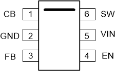
 Figure 5-1 6-Pin SOT-23DBV Package(Top View)
Table 5-1 Pin Functions
| PIN | TYPE(1) | DESCRIPTION | |
|---|---|---|---|
| NAME | NO | ||
| CB | 1 | P | Bootstrap capacitor connection for high-side FET driver. Connect a high quality 100nF capacitor from this pin to the SW pin. |
| GND | 2 | G | Power ground pins. Connected to the source of low-side FET internally. Connect to system ground, ground side of CIN and COUT. The path to CIN must be as short as possible. |
| FB | 3 | A | Feedback input to the converter. Connect a resistor divider to set the output voltage. Connect to Vout directly for fixed output. Never short this terminal to ground during operation. |
| EN | 4 | A | Precision enable input to the converter. Do not float. High = On, Low = Off. Can be tied to VIN. Precision enable input allows an adjustable undervoltage lockout (UVLO) by an external resistor divider. |
| VIN | 5 | P | Supply input pin to the internal bias LDO and high-side FET. Connect to the input supply and input bypass capacitors CIN. Input bypass capacitors must be directly connected to this pin and GND. |
| SW | 6 | P | Switching output of the converter. Internally connected to source of the high-side FET and drain of the low-side FET. Connect to the power inductor. |
(1) A = Analog, P = Power, G = Ground