SLUSF64A August   2024  – November 2024 LMR51635

PRODUCTION DATA  

  1.   1
  2. Features
  3. Applications
  4. Description
  5. Device Comparison Table
  6. Pin Configuration and Functions
  7. Specifications
    1. 6.1 Absolute Maximum Ratings
    2. 6.2 ESD Ratings
    3. 6.3 Recommended Operating Conditions
    4. 6.4 Thermal Information
    5. 6.5 Electrical Characteristics
    6. 6.6 Typical Characteristics
  8. Detailed Description
    1. 7.1 Overview
    2. 7.2 Functional Block Diagram
    3. 7.3 Feature Description
      1. 7.3.1 Fixed Frequency Peak Current Mode Control
      2. 7.3.2 Adjustable Output Voltage
      3. 7.3.3 Enable
      4. 7.3.4 Minimum ON Time, Minimum OFF Time, and Frequency Foldback
      5. 7.3.5 Bootstrap Voltage
      6. 7.3.6 Overcurrent and Short-Circuit Protection
      7. 7.3.7 Soft Start
      8. 7.3.8 Thermal Shutdown
    4. 7.4 Device Functional Modes
      1. 7.4.1 Shutdown Mode
      2. 7.4.2 Active Mode
      3. 7.4.3 CCM Mode
      4. 7.4.4 Light Load Operation (PFM Version)
  9. Application and Implementation
    1. 8.1 Application Information
    2. 8.2 Typical Application
      1. 8.2.1 Design Requirements
      2. 8.2.2 Detailed Design Procedure
        1. 8.2.2.1 Custom Design With WEBENCH® Tools
        2. 8.2.2.2 Output Voltage Set-Point
        3. 8.2.2.3 Switching Frequency
        4. 8.2.2.4 Inductor Selection
        5. 8.2.2.5 Output Capacitor Selection
        6. 8.2.2.6 Input Capacitor Selection
        7. 8.2.2.7 Bootstrap Capacitor
        8. 8.2.2.8 Undervoltage Lockout Set-Point
      3. 8.2.3 Application Curves
    3. 8.3 Power Supply Recommendations
    4. 8.4 Layout
      1. 8.4.1 Layout Guidelines
        1. 8.4.1.1 Compact Layout for EMI Reduction
        2. 8.4.1.2 Feedback Resistors
      2. 8.4.2 Layout Example
  10. Device and Documentation Support
    1. 9.1 Device Support
      1. 9.1.1 Third-Party Products Disclaimer
      2. 9.1.2 Development Support
        1. 9.1.2.1 Custom Design With WEBENCH® Tools
    2. 9.2 Documentation Support
      1. 9.2.1 Related Documentation
    3. 9.3 Receiving Notification of Documentation Updates
    4. 9.4 Support Resources
    5. 9.5 Trademarks
    6. 9.6 Electrostatic Discharge Caution
    7. 9.7 Glossary
  11. 10Revision History
  12. 11Mechanical, Packaging, and Orderable Information

Package Options

Mechanical Data (Package|Pins)
Thermal pad, mechanical data (Package|Pins)
Orderable Information

Enable

The voltage on the EN pin controls the ON, OFF operation of the LMR51635. A voltage of less than 0.88V shuts down the device, while a voltage of greater than 1.35V is required to start the converter. The EN pin is an input and cannot be left open or floating. The simplest way to enable the operation of the LMR51635 is to connect EN to VIN. This connection allows self-start-up of the LMR51635 when VIN is within the operating range.

Many applications benefit from the employment of an enable divider, RENT and RENB (Figure 7-3) to establish a precision system UVLO level for the converter. A system UVLO can be used for supplies operating from utility power as well as battery power. A system UVLO can be used for sequencing, making sure of reliable operation, or supplying protection, such as a battery discharge level. An external logic signal can also be used to drive the EN input for system sequencing and protection.
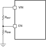
Note: The EN pin voltage must not to be greater than VIN + 0.3V. TI does not recommend to apply EN voltage when VIN is 0V.
LMR51635  System UVLO by Enable DividerFigure 7-3 System UVLO by Enable Divider