SNAS714C November 2016 – August 2021 LMS3635-Q1 , LMS3655-Q1
PRODUCTION DATA
- 1 Features
- 2 Applications
- 3 Description
- 4 Revision History
- 5 Device Comparison Tables
- 6 Pin Configuration and Functions
- 7 Specifications
- 8 Detailed Description
-
9 Application and Implementation
- 9.1 Application Information
- 9.2
Typical Applications
- 9.2.1
General Application
- 9.2.1.1 Design Requirements
- 9.2.1.2 Detailed Design Procedure
- 9.2.1.3 Application Curves
- 9.2.2 Fixed 5-V Output for USB-Type Applications
- 9.2.3 Fixed 3.3-V Output
- 9.2.4 6-V Adjustable Output
- 9.2.1
General Application
- 9.3 Do's and Don't's
- 10Power Supply Recommendations
- 11Layout
- 12Device and Documentation Support
- 13Mechanical, Packaging, and Orderable Information
Package Options
Mechanical Data (Package|Pins)
- RNL|22
Thermal pad, mechanical data (Package|Pins)
- RNL|22
Orderable Information
8.3.1 RESET Flag Output
While the LMS36x5-Q1 reset function resembles a standard Power-Good function, its functionality is designed to replace a discrete reset device, reducing additional component cost. There are three major differences between the reset function and the normal power good function seen in most regulators.
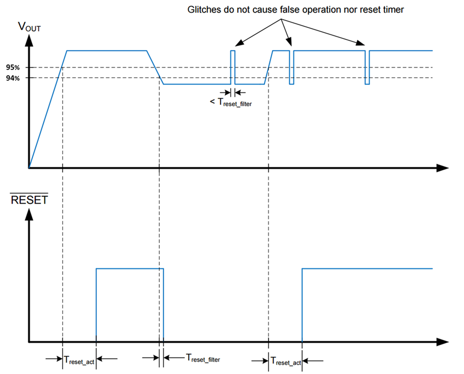
- A delay has been added between the point at which the output voltage is within specified limits and the flag asserts Power Good. A glitch filter prevents false flag operation for short excursions in the output voltage, such as during line and load transients. See Figure 8-3 and Figure 8-4 for more detail.
- RESET output signals a fault (pulls its output to ground) while the part is disabled.
- RESET continues to operate with input voltage as low as 1.5 V. Below this input voltage, RESET output may be high impedance.
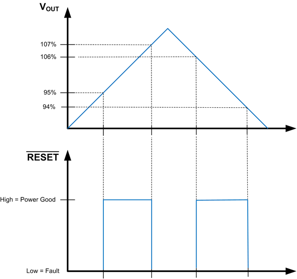
Because the RESET comparator and the regulation loop share the same reference, the thresholds track with the output voltage. When EN is pulled low, the RESET flag output is forced low. When the device is disabled, RESET remains valid as long as the input voltage is ≥ 1.5 V. RESET operation can best be understood by reference to Figure 8-2 and Figure 8-3. Output voltage excursions lasting less than TRESET-filter do not trip RESET. Once the output voltage is within the prescribed limits, a delay of TRESET-act is imposed before RESET goes high. This enables tighter tolerance than is possible with an external supervisor device while also expanding the system allowance for transient response without the need for extremely accurate internal circuitry.
This output consists of an open-drain NMOS; requiring an external pullup resistor to a suitable logic supply. It can also be pulled up to either VCC or VOUT, through an appropriate resistor, as desired. The pin can be left floating or grounded if the RESET function is not used in the application. The maximum current into this pin must be limited to 10 mA, and the maximum voltage must be less than 8 V.
 Figure 8-2 Static
RESET Operation
 Figure 8-3 RESET Timing Behavior
The threshold voltage for the RESET function takes advantage of the availability of the LMS36x5-Q1 internal feedback threshold to the RESET circuit. This allows a maximum threshold of 96.5% of selected output voltage to be specified at the same time as 96% of actual set point.