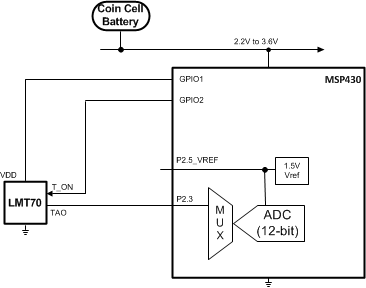
The LMT70 is an ultra-small, high-precision, low-power CMOS analog temperature sensor with an output enable pin. Applications for the LMT70 include virtually any type of temperature sensing where cost-effective, high precision and low-power are required, such as Internet of Things (IoT) sensor nodes, medical thermometers, high-precision instrumentation and battery powered devices. The LMT70 is also a great replacement for RTD and precision NTC/PTC thermistors.
Its output enable pin allows multiple LMT70s to share one ADC channel, thus simplifying ADC calibration and reducing the overall system cost for precision temperature sensing. The LMT70 also has a linear and low impedance output allowing seamless interface to an off-the-shelf MCU/ADC. Dissipating less than 36µW, the LMT70 has ultra-low self-heating supporting its high-precision over a wide temperature range.
The LMT70A provides unparalleled temperature matching performance of 0.1°C (max) for two adjacent LMT70A's picked from the same tape and reel. Therefore, the LMT70A is an ideal solution for energy metering applications requiring heat transfer calculations.
PART NUMBER | PACKAGE | BODY SIZE (NOM) |
---|---|---|
LMT70 | DSBGA - WLCSP (4) YFQ | 0.88 mm x 0.88 mm |
Changes from * Revision (March 2015) to A Revision
Order Number | Matching Specification Provided(1) |
---|---|
LMT70YFQR, LMT70YFQT | No |
LMT70AYFQR, LMT70AYFQT | Yes, 0.1°C at approximately 30°C(1) |
MIN | MAX | UNIT | ||
---|---|---|---|---|
Supply voltage | −0.3 | 6 | V | |
Voltage at T_ON and TAO | −0.3 | 6 | V | |
Current at any pin | 5 | mA | ||
Storage temperature, Tstg | -65 | 150 | °C |
VALUE | UNIT | |||
---|---|---|---|---|
V(ESD) | Electrostatic discharge | Human-body model (HBM), per ANSI/ESDA/JEDEC JS-001(1) | ±2000 | V |
Charged-device model (CDM), per JEDEC specification JESD22-C101(2) | ±750 |
MIN | NOM | MAX | UNIT | |
---|---|---|---|---|
Specified temperature (TMIN ≤ TA ≤ TMAX) | −55 | 150 | °C | |
Supply voltage | 2.0 | 5.5 | V |
THERMAL METRIC(1) | LMT70 | UNIT | |
---|---|---|---|
DSBGA or WLCSP | |||
YFQ 4 PINS | |||
RθJA | Junction-to-ambient thermal resistance | 187 | °C/W |
RθJC(top) | Junction-to-case (top) thermal resistance | 2.3 | |
RθJB | Junction-to-board thermal resistance | 105 | |
ψJT | Junction-to-top characterization parameter | 10.9 | |
ψJB | Junction-to-board characterization parameter | 104 | |
Thermal response time to 63% of final value in stirred oil (dominated by PCB see layout) | 1.5 | sec | |
Thermal response time to 63% of final value in still air (dominated by PCB see layout) | 73 | sec |
PARAMETER | TEST CONDITIONS | MIN | TYP | MAX | UNIT | ||
---|---|---|---|---|---|---|---|
TEMPERATURE ACCURACY | |||||||
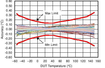
TAO accuracy (These stated accuracy limits are with reference to the values in Electrical Characteristics Temperature Lookup Table (LUT), LMT70 temperature-to-voltage.)(1) |
TA = –55°C | VDD = 2.7 V | -0.33 | 0.33 | °C | ||
TA = –40°C | VDD = 2.7 V | –0.27 | 0.27 | ||||
TA = –20°C | VDD = 2.7 V | –0.2 | 0.2 | ||||
TA = –10°C | VDD = 2.7 V | –0.18 | 0.18 | ||||
TA = 20°C to 42°C | VDD = 2.7 V | –0.13 | ±0.05 | 0.13 | |||
TA = 50°C | VDD = 2.7 V | -0.15 | 0.15 | ||||
TA = 90°C | VDD = 2.7 V | –0.20 | 0.20 | ||||
TA = 110°C | VDD = 2.7 V | –0.23 | 0.23 | ||||
TA = 150°C | VDD = 2.7 V | –0.36 | 0.36 | ||||
ATC | Accuracy temperature coefficient (note, uses end point calculations)(2) | VDD = 2.7V | -2.6 | +2.6 | m°C/°C | ||
APSS | Accuracy power supply sensitivity (note uses end point calculations) | –55°C ≤ TA ≤ 10°C | VDD = VTAO + 1.1 V to 4.0 V | –9 | –2 | 8 | m°C /V |
10°C ≤ TA ≤ 120°C | VDD = 2.0 V to 4.0 V | ||||||
120°C ≤ TA ≤ 150°C | VDD = 2.0 V to 4.0 V | –15 | 8 | ||||
VDD = 4 V to 5.5 V | –30 | –12 | 0 | ||||
VTAO | Output Voltage | TA = 30°C | VDD = 2.7 V | 943.227 | mV | ||
Sensor gain | –5.194 | mV/°C | |||||
Matching of two adjacent parts in tape and reel for LMT70AYFQR, LMT70AYFQT only (see curve Figure 19 for specification at other temperatures)(3)(2) | TA approximately 30°C | VDD = 2.0 V to 3.6 V | 0.1 | °C | |||
TA = 30°C to 150°C | 2.5 | m°C /°C | |||||
TA = 20°C to 30°C | VDD = 2.0 V to 3.6 V | -2.5 | |||||
TA = -55°C to 30°C | VDD = 2.7 V to 3.6 V | –2.5 | |||||
Time stability(4) | 10k hours at 90°C | –0.1 | ±0.01 | 0.1 | °C | ||
ANALOG OUTPUT | |||||||
Operating output voltage change with load current | 0 µA≤IL≤5 µA | 0 | 0.4 | mV | |||
-5 µA≤IL≤0 µA | -0.4 | 0 | mV | ||||
ROUT | Output Resistance | 28 | 80 | Ω | |||
TAO Off Leakage Current | VTAO ≤ VDD – 0.6v, VT_ON=GND | 0.005 | 0.5 | µA | |||
VTAO ≥ 0.2V, VT_ON = GND | -0.5 | -0.005 | |||||
Output Load Capacitance | 1100 | pF | |||||
POWER SUPPLY | |||||||
VDO | Dropout Voltage (VDD-VTAO)(5) | –20°C ≤ TA ≤ 20°C | 1.0 | V | |||
–55°C ≤ TA ≤ –20°C | 1.1 | ||||||
Power Supply Current | 9.2 | 12 | µA | ||||
Shutdown Current | VDD ≤ 0.4V (-55°C to +110°C) | 50 | nA | ||||
VDD ≤ 0.4V (+110°C to +150°C) | 350 | nA | |||||
LOGIC INPUT | |||||||
T_ON Logic Low Input Threshold | -55°C to +150°C | 0.5 | 0.33*VDD | V | |||
T_ON Logic High Input Threshold | -55°C to +150°C | 0.66*VDD | VDD-0.5 | V | |||
T_ON Input Current | VT_ON = VDD | 0.15 | 1 | µA | |||
VT_ON = GND | -1 | -0.02 |
PARAMETER | TEST CONDITIONS | MIN | TYP | MAX | UNIT | |
---|---|---|---|---|---|---|
tPOWER | Power-on Time to 99% of final voltage value | CL=0 pF to 1100 pF; VDD connected T_ON | 0.6 | 1 | ms | |
tT_ON | T_ON Time to 99% of final voltage value (note dependent on RON and C load) | CL=150pF | 30 | 500 | µs | |
CT_ON | T_ON Digital Input Capacitance | 2.2 | pF |
VDD=2.7V | ||
using LUT (Look-Up Table) and linear interporlation for conversion of voltage to temperature |
VDD=2.7V | ||
using LUT table for conversion of voltage to temperature |
VDD=2.7V | ||
using LUT table for conversion of voltage to temperature |
VDD=2.7V | ||
using LUT table for conversion of voltage to temperature |
VDD=2.7V | ||
using LUT table for conversion of voltage to temperature |
VDD=2.7V | ||
using LUT table for conversion of voltage to temperature |
Conditions: | Various VDD and CLOAD | ||
VDD=2.7V | ||
using LUT table for conversion of voltage to temperature |
VDD=2.7V | ||
using LUT table for conversion of voltage to temperature |
VDD=2.7V | ||
using LUT table for conversion of voltage to temperature |
VDD=2.7V | ||
using LUT table for conversion of voltage to temperature |
VDD=2.7V | ||
using LUT table for conversion of voltage to temperature |
VDD=2.7V | ||
using LUT table for conversion of voltage to temperature |
VDD=2.7V | ||
VDD=3.3V | ||
Top trace is T_ON | ||
Bottom trace is TAO |
at various temperatures | ||