SNIS187A March 2015 – July 2015 LMT70 , LMT70A
PRODUCTION DATA.
- 1 Features
- 2 Applications
- 3 Description
- 4 Wide-Range Precision Active RTD or NTC Replacement (−55°C to 150°C)
- 5 Revision History
- 6 Device Comparison Table
- 7 Pin Configuration and Functions
- 8 Specifications
- 9 Detailed Description
- 10Application and Implementation
- 11Power Supply Recommendations
- 12Layout
- 13Device and Documentation Support
- 14Mechanical, Packaging, and Orderable Information
Package Options
Mechanical Data (Package|Pins)
- YFQ|4
Thermal pad, mechanical data (Package|Pins)
Orderable Information
9 Detailed Description
9.1 Overview
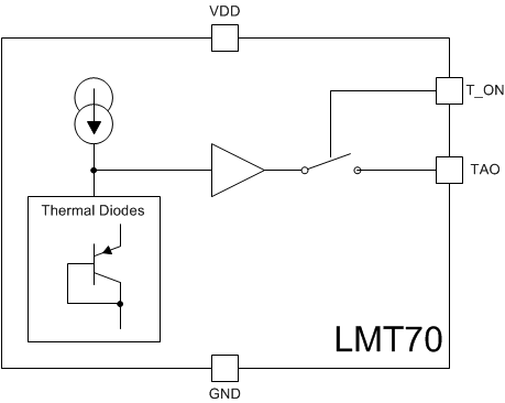
The LMT70 is a precision analog output temperature sensor. It includes an output switch that is controlled by the T_ON digital input. The output switch enables the multiplexing of several devices onto a single ADC input thus expanding on the ADC input multiplexer capability.
The temperature sensing element is comprised of simply stacked BJT base emitter junctions that are biased by a current source. The temperature sensing element is then buffered by a precision amplifier before being connected to the output switch. The output amplifier has a simple class AB push-pull output stage that enables the device to easily source and sink current.
9.2 Functional Block Diagram

9.3 Feature Description
9.3.1 Temperature Analog Output (TAO)
The TAO push-pull output provides the ability to sink and source current. This is beneficial when, for example, driving dynamic loads like an input stage on an analog-to-digital converter (ADC). In these applications the source current is required to quickly charge the input capacitor of the ADC. See the Typical Application section for more discussion of this topic. The LMT70 is ideal for this and other applications which require strong source or sink current.
9.3.1.1 LMT70 Output Transfer Function
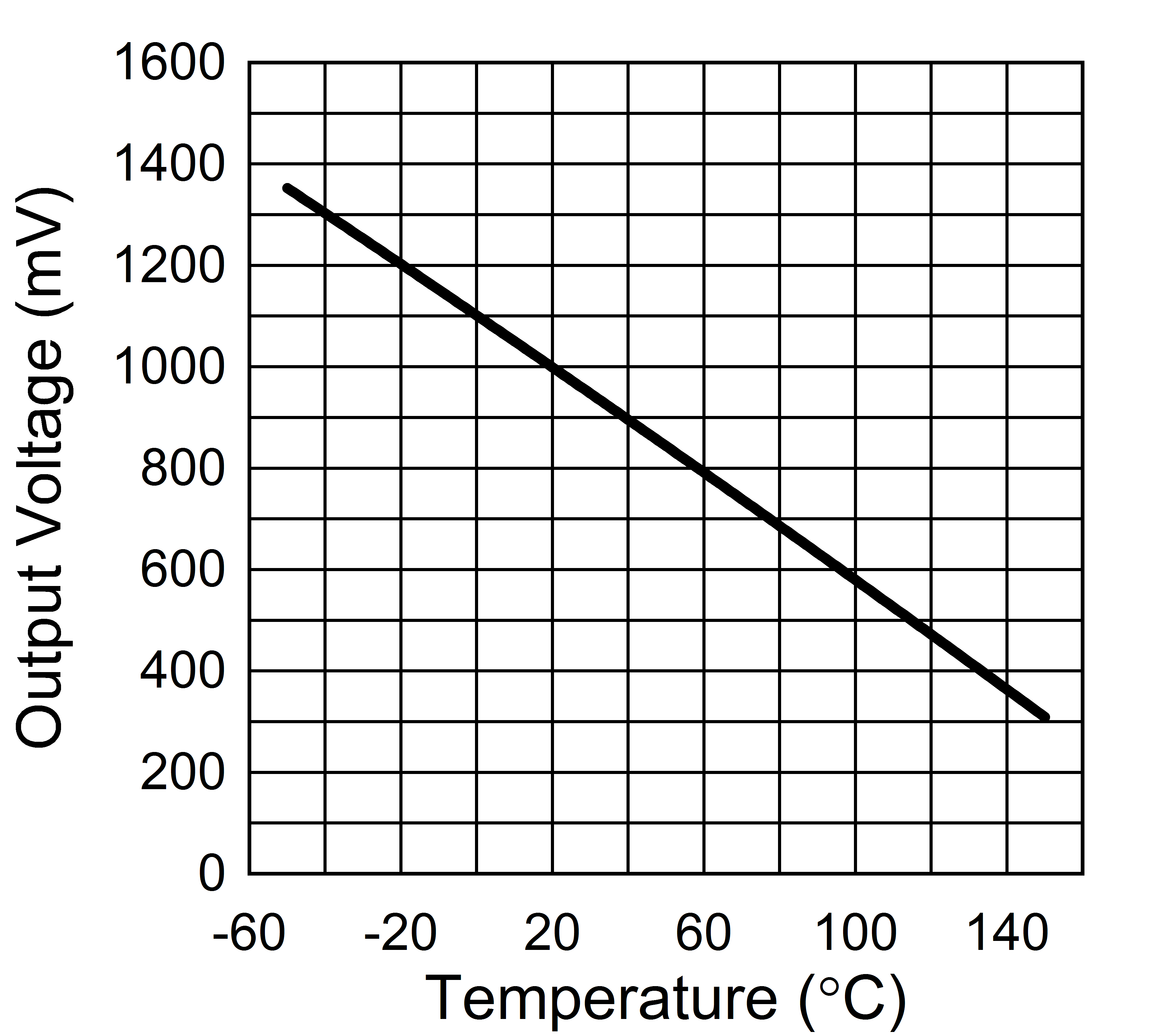
The LMT70 output voltage transfer function appears to be linear, but upon close inspection it can be seen that it is truly not linear and can be better described by a second or third order transfer function equation.
 Figure 23. LMT70 Output Transfer Function
9.3.1.1.1 First Order Transfer Function
A first order transfer function can be used to calculate the temperature LMT70 is sensing but over a wide temperature range it is the least accurate method. An equation can be easily generated using the LUT (Look-Up Table) information found in Electrical Characteristics Temperature Lookup Table (LUT) .
Over a narrow 10°C temperature range a linear equation will yield very accurate results. It is actually recommended that over a 10°C temperature range linear interpolation be used to calculate the temperature the device is sensing. When this method is used the accuracy minimum and maximum specifications would meet the values given in Figure 3.
For example the first order equation between 20°C and 30°C can be generated using the typical output voltage levels as given in Electrical Characteristics Temperature Lookup Table (LUT) and partially repeated here for reference from 20°C to 50°C:
Table 1. Output Voltage LUT
| Temperature (°C) | VTAO (mV) | Local Slope (mV/°C) | ||
|---|---|---|---|---|
| MIN | TYP | MAX | ||
| 20 | 994.367 | 995.050 | 995.734 | -5.171 |
| 30 | 942.547 | 943.227 | 943.907 | -5.194 |
| 40 | 890.423 | 891.178 | 891.934 | -5.217 |
| 50 | 838.097 | 838.882 | 839.668 | -5.241 |
First calculate the slope:
m =(T1 – T2) ÷ [(VTAO (T1) – VTAO (T2)]
m = (20°C - 30°C) ÷ (995.050 mV – 943.227 mV)
m = –0.193 °C/mV
Then calculate the y intercept b:
b = (T1) – (m × VTAO(T1))
b = 20°C – (–0.193 °C/mV × 995.050 mV)
b = 212.009°C
Thus the final equation used to calculate the measured temperature (TM) in the range between 20°C and 30°C is:
TM = m × VTAO + b
TM = –0.193 °C/mV × VTAO + 212.009°C
where VTAO is in mV and TM is in °C.
9.3.1.1.2 Second Order Transfer Function
A second order transfer function can give good results over a wider limited temperature range. Over the full temperature range of -55°C to +150°C a single second order transfer function will have increased error at the temperature extremes. Using least squares sum method a best fit second order transfer function was generated using the values in Electrical Characteristics Temperature Lookup Table (LUT):
TM = a (VTAO)2+ b (VTAO) + c
where:
| Best fit for -55°C to 150°C | Best fit for -10°C to 110°C | |
|---|---|---|
| a | -8.451576E-06 | -7.857923E-06 |
| b | -1.769281E-01 | -1.777501E-01 |
| c | 2.043937E+02 | 2.046398E+02 |
and VTAO is in mV and TM is in °C.
9.3.1.1.3 Third Order Transfer Function
Over a wide temperature range the most accurate single equation is a third order transfer function. Using least squares sum method a best fit third order transfer function was generated using the values in Figure 3:
TM = a (VTAO)3 + b (VTAO)2 + c(VTAO) + d
where:
| Best fit for -55°C to 150°C | Best fit for -10°C to 110°C | |
|---|---|---|
| a | -1.064200E-09 | -1.809628E-09 |
| b | -5.759725E-06 | -3.325395E-06 |
| c | -1.789883E-01 | -1.814103E-01 |
| d | 2.048570E+02 | 2.055894E+02 |
and VTAO is in mV and TM is in °C.
9.3.1.2 LMT70A TAO Matching
In order to meet the matching specification of the LMT70A, two units must be picked from adjacent positions from one tape and reel. If PCB rework is required, involving the LMT70A, then the pair of the LMT70A matched units must be replaced. Matching features (which include, without limitation, electrical matching characteristics of adjacent Components as they are delivered in original packaging from TI) are warranted solely to the extent that the purchaser can demonstrate to TI’s satisfaction that the particular Component(s) at issue were adjacent in original packaging as delivered by TI. Customers should be advised that the small size of these components means they are not individually traceable at the unit level and it may be difficult to establish the original position of the Components once they have been removed from that original packaging as delivered by TI.
9.3.1.3 TAO Noise Considerations
A load capacitor on TAO pin can help to filter noise.
For noisy environments, TI recommends at minimum 100 nF supply decoupling capacitor placed close across VDD and GND pins of LMT70.
9.3.1.4 TAO Capacitive Loads
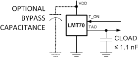
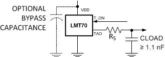
TAO handles capacitive loading well. In an extremely noisy environment, or when driving a switched sampling input on an ADC, it may be necessary to add some filtering to minimize noise coupling. Without any precautions, the VTAO can drive a capacitive load less than or equal to 1 nF as shown in Figure 24. For capacitive loads greater than 1 nF, a series resistor is required on the output, as shown in Figure 25, to maintain stable conditions.
 Figure 24. LMT70 No Isolation Resistor Required
 Figure 25. LMT70 With Series Resistor for Capacitive Loading Greater than 1 nF
Table 2. CLOAD and RS Values of Figure 25
| CLOAD | Minimum RS |
|---|---|
| 1.1 to 90 nF | 3 kΩ |
| 90 to 900 nF | 1.5 kΩ |
| 0.9 μF | 750 Ω |
9.3.2 TON Digital Input
The T_ON digital input enables and disables the analog output voltage presented at the TAO pin by controlling the state of the internal switch that is in series with the internal temperature sensor circuitry output. When T_ON is driven to a logic "HIGH" the temperature sensor output voltage is present on the TAO pin. When T_ON is set to a logic "LOW" the TAO pin is set to a high impedance state.
9.3.3 Light Sensitivity
Although the LMT70 package has a protective backside coating that reduces the amount of light exposure on the die, unless it is fully shielded, ambient light will still reach the active region of the device from the side of the package. Depending on the amount of light exposure in a given application, an increase in temperature error should be expected. In circuit board tests under ambient light conditions, a typical increase in error may not be observed and is dependent on the angle that the light approaches the package. The LMT70 is most sensitive to IR radiation. Best practice should include end-product packaging that provides shielding from possible light sources during operation.
9.4 Device Functional Modes
The LMT70 is a simple precise analog output temperature sensor with a switch in series with its output. It has only two functional modes: output on or output off.