SLOSE67D
june 2020 – april 2023
LMV321A-Q1
,
LMV324A-Q1
,
LMV358A-Q1
PRODUCTION DATA
1
Features
2
Applications
3
Description
4
Revision History
5
Pin Configuration and Functions
6
Specifications
6.1
Absolute Maximum Ratings
6.2
ESD Ratings
6.3
Recommended Operating Conditions
6.4
Thermal Information: LMV321A-Q1
6.5
Thermal Information: LMV358A-Q1
6.6
Thermal Information: LMV324A-Q1
6.7
Electrical Characteristics
6.8
Typical Characteristics
7
Detailed Description
7.1
Overview
7.2
Functional Block Diagram
7.3
Feature Description
7.3.1
Operating Voltage
7.3.2
Input Common Mode Range
7.3.3
Rail-to-Rail Output
7.3.4
Overload Recovery
7.4
Device Functional Modes
8
Application and Implementation
8.1
Application Information
8.2
Typical Application
8.2.1
LMV3xxA-Q1 Low-Side, Current Sensing Application
8.2.1.1
Design Requirements
8.2.1.2
Detailed Design Procedure
8.2.1.3
Application Curve
8.2.2
Single-Supply Photodiode Amplifier
8.2.2.1
Design Requirements
8.2.2.2
Detailed Design Procedure
8.2.2.3
Application Curves
9
Power Supply Recommendations
9.1
Input and ESD Protection
10
Layout
10.1
Layout Guidelines
10.2
Layout Example
11
Device and Documentation Support
11.1
Documentation Support
11.1.1
Related Documentation
11.2
Receiving Notification of Documentation Updates
11.3
Support Resources
11.4
Trademarks
11.5
Electrostatic Discharge Caution
11.6
Glossary
12
Mechanical, Packaging, and Orderable Information
Package Options
Mechanical Data (Package|Pins)
DYY|14
MPSS114C
PW|14
MPDS360A
D|14
MPDS177H
Thermal pad, mechanical data (Package|Pins)
Orderable Information
slose67d_oa
slose67d_pm
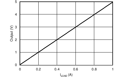
8.2.1.3
Application Curve
Figure 8-2
Low-Side, Current-Sense Transfer Function