SBOS923I December 2017 – July 2024 LMV321A , LMV324A , LMV358A
PRODUCTION DATA
- 1
- 1 Features
- 2 Applications
- 3 Description
- 4 Pin Functions and Configurations
- 5 Specifications
- 6 Detailed Description
- 7 Application and Implementation
- 8 Device and Documentation Support
- 9 Revision History
- 10Mechanical, Packaging, and Orderable Information
Package Options
Mechanical Data (Package|Pins)
Thermal pad, mechanical data (Package|Pins)
Orderable Information
3 Description
The LMV3xxA family includes single (LMV321A), dual (LMV358A), and quad-channel (LMV324A) low-voltage (2.5V to 5.5V) operational amplifiers (op amps) with rail-to-rail output swing capabilities. These op amps provide a cost-effective solution for space-constrained applications such as large appliances, smoke detectors, and personal electronics where low-voltage operation and high capacitive-load drive are required. The capacitive-load drive of the LMV3xxA family is 500pF, and the resistive open-loop output impedance makes stabilization easier with much higher capacitive loads. These op amps are designed specifically for low-voltage operation (2.5V to 5.5V) with performance specifications similar to the LMV3xx devices.
The robust design of the LMV3xxA family simplifies circuit design. The op amps feature unity-gain stability, an integrated RFI and EMI rejection filter, and no-phase reversal in overdrive conditions.
The LMV3xxA family is available in industry-standard packages such as SOIC, MSOP, SOT-23, and TSSOP packages.
| PART NUMBER | PACKAGE(1) | PACAKGE SIZE(2) |
|---|---|---|
| LMV321A | DBV (SOT-23, 5) | 2.9mm × 2.8mm |
| DCK (SC70, 5) | 2mm × 2.1mm | |
| LMV358A | D (SOIC, 8) | 4.9mm × 6mm |
| DGK (VSSOP, 8) | 3mm × 4.9mm | |
| PW (TSSOP, 8) | 3mm × 6.4mm | |
| DDF (SOT-23, 8) | 2.9mm × 2.8mm | |
| LMV324A | D (SOIC, 14) | 8.65mm × 6mm |
| DYY (SOT-23, 14) | 4.2mm × 3.26mm | |
| PW (TSSOP, 14) | 5mm × 6.4mm |
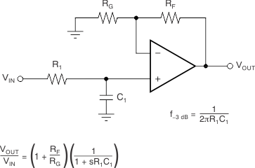
 Single-Pole, Low-Pass Filter