-
LMV61x Single, Dual, and Quad, 1.4-MHz, Low-Power, General-Purpose 1.8-V Operational Amplifiers
- 1 Features
- 2 Applications
- 3 Description
- 4 Revision History
- 5 Pin Configuration and Functions
-
6 Specifications
- 6.1 Absolute Maximum Ratings
- 6.2 ESD Ratings
- 6.3 Recommended Operating Conditions
- 6.4 Thermal Information
- 6.5 Electrical Characteristics - 1.8 V (DC)
- 6.6 Electrical Characteristics - 1.8 V (AC)
- 6.7 Electrical Characteristics - 2.7 V (DC)
- 6.8 Electrical Characteristics - 2.7 V (AC)
- 6.9 Electrical Characteristics - 5 V (DC)
- 6.10 Electrical Characteristics - 5 V (AC)
- 6.11 Typical Characteristics
- 7 Detailed Description
- 8 Application and Implementation
- 9 Power Supply Recommendations
- 10Layout
- 11Device and Documentation Support
- 12Mechanical, Packaging, and Orderable Information
- IMPORTANT NOTICE
Package Options
Mechanical Data (Package|Pins)
Thermal pad, mechanical data (Package|Pins)
Orderable Information
LMV61x Single, Dual, and Quad, 1.4-MHz, Low-Power, General-Purpose 1.8-V Operational Amplifiers
1 Features
- Supply Values: 1.8 V (Typical)
- Ensured 1.8-V, 2.7-V, and 5-V Specifications
- Output Swing:
- 80 mV From Rail With 600-Ω Load
- 30 mV From Rail With 2-kΩ Load
- VCM = 200 mV Beyond Rails
- 100-µA Supply Current (Per Channel)
- 1.4-MHz Gain Bandwidth Product
- Maximum VOS = 4 mV
- Temperature Range: −40°C to +125°C
- Create a Custom Design Using the LMV61x With the WEBENCH® Power Designer
2 Applications
- Consumer Communication
- Consumer Computing
- PDAs
- Audio Pre-Amplifiers
- Portable or Battery-Powered Electronic Equipment
- Supply Current Monitoring
- Battery Monitoring
Typical Application
3 Description
The LMV61x devices are single, dual, and quad low-voltage, low-power operational amplifiers (op amps). They are designed specifically for low-voltage, general-purpose applications. Other important product characteristics are, rail-to-rail input or output, low supply voltage of 1.8 V and wide temperature range. The LMV61x input common mode extends
200 mV beyond the supplies and the output can swing rail-to-rail unloaded and within 30 mV with 2-kΩ load at 1.8-V supply. The LMV61x achieves a gain bandwidth of 1.4 MHz while drawing 100-µA (typical) quiescent current.
The industrial-plus temperature range of −40°C to 125°C allows the LMV61x to accommodate a broad range of extended environment applications.
The LMV611 is offered in the tiny 5-pin SC70 package, the LMV612 in space-saving 8-pin VSSOP and SOIC packages, and the LMV614 in 14-pin TSSOP and SOIC packages. These small package amplifiers offer an ideal solution for applications requiring minimum PCB footprint. Applications with area constrained PCB requirements include portable and battery-operated electronics.
Device Information(1)
| PART NUMBER | PACKAGE | BODY SIZE (NOM) |
|---|---|---|
| LMV611 | SOT-23 (5) | 2.92 mm × 1.60 mm |
| SC70 (5) | 2.00 mm × 1.25 mm | |
| LMV612 | VSSOP (8) | 3.00 mm × 3.00 mm |
| SOIC (8) | 4.90 mm × 3.91 mm | |
| LMV614 | TSSOP (14) | 5.00 mm × 4.40 mm |
| SOIC (14) | 8.64 mm × 3.90 mm |
- For all available packages, see the orderable addendum at the end of the data sheet.
4 Revision History
Changes from C Revision (July 2016) to D Revision
- Added links for WEBENCH Go
- Changed Slew Rate vs Supply title to reflect LMV611 and LMV614 onlyGo
- Added Slew Rate vs Supply Graph for LMV612 only Go
Changes from B Revision (March 2013) to C Revision
- Added ESD Ratings table, Feature Description section, Device Functional Modes, Application and Implementation section, Power Supply Recommendations section, Layout section, Device and Documentation Support section, and Mechanical, Packaging, and Orderable Information sectionGo
- Changed values in the Thermal Information table to align with JEDEC standardsGo
Changes from A Revision (March 2012) to B Revision
- Changed layout of National Semiconductor data sheet to TI formatGo
5 Pin Configuration and Functions

Pin Functions – LMV611
| PIN | TYPE(1) | DESCRIPTION | |
|---|---|---|---|
| NO. | NAME | ||
| 1 | +IN | I | Noninverting input |
| 2 | V– | P | Negative supply input |
| 3 | –IN | I | Inverting input |
| 4 | OUTPUT | O | Output |
| 5 | V+ | P | Positive supply input |

Pin Functions – LMV612
| PIN | TYPE(1) | DESCRIPTION | |
|---|---|---|---|
| NO. | NAME | ||
| 1 | OUT A | O | Output A |
| 2 | –IN A | I | Inverting input A |
| 3 | +IN A | I | Noninverting input A |
| 4 | V– | P | Negative supply input |
| 5 | +IN B | I | Noninverting input B |
| 6 | –IN B | I | Inverting input B |
| 7 | OUT B | O | Output B |
| 8 | V+ | P | Positive supply input |

Pin Functions – LMV614
| PIN | TYPE(1) | DESCRIPTION | |
|---|---|---|---|
| NO. | NAME | ||
| 1 | OUT A | O | Output A |
| 2 | IN A– | I | Inverting input A |
| 3 | IN A+ | I | Noninverting input A |
| 4 | V+ | P | Positive supply input |
| 5 | IN B+ | I | Noninverting input B |
| 6 | IN B– | I | Inverting input B |
| 7 | OUT B | O | Output B |
| 8 | OUT C | O | Output C |
| 9 | IN C– | I | Inverting input C |
| 10 | IN C+ | I | Noninverting input C |
| 11 | V– | P | Negative supply input |
| 12 | IN D+ | I | Noninverting input D |
| 13 | IN D– | I | Inverting input D |
| 14 | OUT D | O | Output D |
6 Specifications
6.1 Absolute Maximum Ratings
over operating free-air temperature range (unless otherwise noted)(1)(2)(3)| MIN | MAX | UNIT | |
|---|---|---|---|
| Differential input voltage | ±Supply voltage | ||
| Supply voltage (V+–V −) | 6 | V | |
| Voltage at input or output pin | V– – 0.3 | V++ 0.3 | V |
| Junction temperature, TJMAX(4) | 150 | °C | |
| Storage temperature, Tstg | –65 | 150 | °C |
6.2 ESD Ratings
| VALUE | UNIT | |||
|---|---|---|---|---|
| V(ESD) | Electrostatic discharge | Human-body model (HBM), per ANSI/ESDA/JEDEC JS-001(1) | ±2000 | V |
| Machine model (MM)(2) | ±200 | |||
6.3 Recommended Operating Conditions
over operating free-air temperature range (unless otherwise noted)| MIN | MAX | UNIT | |
|---|---|---|---|
| Supply voltage | 1.8 | 5.5 | V |
| Temperature | –40 | 125 | °C |
6.4 Thermal Information
| THERMAL METRIC(1) | LMV611 | LMV612 | LMV614 | UNIT | ||||
|---|---|---|---|---|---|---|---|---|
| DBV (SOT-23) |
DCK (SC70) |
D (SOIC) |
DGK (VSSOP) |
D (SOIC) |
PW (TSSOP) |
|||
| 5 PINS | 5 PINS | 8 PINS | 8 PINS | 14 PINS | 14 PINS | |||
| RθJA | Junction-to-ambient thermal resistance | 197.2 | 285.9 | 125.9 | 184.5 | 94.4 | 124.8 | °C/W |
| RθJC(top) | Junction-to-case (top) thermal resistance | 156.7 | 115.9 | 70.2 | 74.3 | 52.5 | 51.4 | °C/W |
| RθJB | Junction-to-board thermal resistance | 55.6 | 63.7 | 66.5 | 105.1 | 48.9 | 67.2 | °C/W |
| ψJT | Junction-to-top characterization parameter | 41.4 | 4.5 | 19.8 | 13.1 | 14.3 | 6.6 | °C/W |
| ψJB | Junction-to-board characterization parameter | 55 | 62.9 | 65.9 | 103.6 | 48.6 | 66.6 | °C/W |
| RθJC(bot) | Junction-to-case (bottom) thermal resistance | — | — | — | — | — | — | °C/W |
6.5 Electrical Characteristics – 1.8 V (DC)
All limits ensured for TJ = 25°C, V+ = 1.8 V, V − = 0 V, VCM = V+/ 2, VO = V+/ 2, and RL > 1 MΩ (unless otherwise noted).(1)| PARAMETER | TEST CONDITIONS | MIN(2) | TYP(3) | MAX(2) | UNIT | ||
|---|---|---|---|---|---|---|---|
| VOS | Input offset voltage | LMV611 (single) | 1 | 4 | mV | ||
| LMV612 (dual) and LMV614 (quad) |
1 | 5.5 | |||||
| TCVOS | Input offset voltage average drift | 5.5 | µV/°C | ||||
| IB | Input bias current | 15 | nA | ||||
| IOS | Input offset current | 13 | nA | ||||
| IS | Supply current (per channel) | 103 | 185 | µA | |||
| CMRR | Common-mode rejection ratio | LMV611, 0 V ≤ VCM ≤ 0.6 V, 1.4 V ≤ VCM ≤ 1.8 V(4) |
60 | 78 | dB | ||
| LMV612 and LMV614, 0 V ≤ VCM ≤ 0.6 V, 1.4 V ≤ VCM ≤ 1.8 V(4) |
55 | 76 | |||||
| −0.2 V ≤ VCM ≤ 0 V, 1.8 V ≤ VCM ≤ 2 V |
50 | 72 | |||||
| PSRR | Power supply rejection ratio | 1.8 V ≤ V+ ≤ 5 V | 100 | dB | |||
| CMVR | Input common-mode voltage | For CMRR range ≥ 50 dB | V–, TA = 25°C | V– – 0.2 | –0.2 | V | |
| V+, TA = 25°C | 2.1 | V+ + 0.2 | |||||
| TA = −40°C to 85°C | V– | V+ | |||||
| TA = 125°C | V– + 0.2 | V+ – 0.2 | |||||
| AV | Large signal voltage gain LMV611 (single) |
RL = 600 Ω to 0.9 V, VO = 0.2 V to 1.6 V, VCM = 0.5 V |
77 | 101 | dB | ||
| RL = 2 kΩ to 0.9 V, VO = 0.2 V to 1.6 V, VCM = 0.5 V |
80 | 105 | |||||
| Large signal voltage gain LMV612 (dual) and LMV614 (quad) |
RL = 600 Ω to 0.9 V, VO = 0.2 V to 1.6 V, VCM = 0.5 V |
75 | 90 | ||||
| RL = 2 kΩ to 0.9 V, VO = 0.2 V to 1.6 V, VCM = 0.5 V |
78 | 100 | |||||
| VO | Output swing | RL = 600 Ω to 0.9 V | 1.65 | 1.72 | V | ||
| VIN = ±100 mV | 0.077 | 0.105 | |||||
| RL = 2 kΩ to 0.9 V | 1.75 | 1.77 | |||||
| VIN = ±100 mV | 0.024 | 0.035 | |||||
| IO | Output short-circuit current(5) | Sourcing, VO = 0 V, VIN = 100 mV |
8 | mA | |||
| Sinking, VO = 1.8 V, VIN = –100 mV |
9 | ||||||
6.6 Electrical Characteristics – 1.8 V (AC)
All limits ensured for TJ = 25°C, V+ = 1.8 V, V − = 0 V, VCM = V+/ 2, VO = V+/ 2, and RL > 1 MΩ (unless otherwise noted).(1)| PARAMETER | TEST CONDITIONS | MIN(2) | TYP(3) | MAX(2) | UNIT | |
|---|---|---|---|---|---|---|
| SR | Slew rate(4) | 0.35 | V/µs | |||
| GBW | Gain-bandwidth product | 1.4 | MHz | |||
| Φm | Phase margin | 67 | ° | |||
| Gm | Gain margin | 7 | dB | |||
| en | Input-referred voltage noise | f = 10 kHz, VCM = 0.5 V | 60 | nV/√Hz | ||
| in | Input-referred current noise | f = 10 kHz | 0.08 | pA/√Hz | ||
| THD | Total harmonic distortion | f = 1 kHz, AV = +1, RL = 600 Ω, VIN = 1 VPP |
0.023% | |||
| Amp-to-amp isolation(5) | 123 | dB | ||||
6.7 Electrical Characteristics – 2.7 V (DC)
All limits ensured for TJ = 25°C, V+ = 2.7 V, V − = 0 V, VCM = V+/ 2, VO = V+/ 2, and RL > 1 MΩ (unless otherwise noted).(1)| PARAMETER | TEST CONDITIONS | MIN(2) | TYP(3) | MAX(2) | UNIT | ||
|---|---|---|---|---|---|---|---|
| VOS | Input offset voltage | LMV611 (single) | 1 | 4 | mV | ||
| LMV612 (dual) and LMV614 (quad) |
1 | 5.5 | |||||
| TCVOS | Input offset voltage average drift | 5.5 | µV/°C | ||||
| IB | Input bias current | 15 | nA | ||||
| IOS | Input offset current | 8 | nA | ||||
| IS | Supply current (per channel) | 105 | 190 | µA | |||
| CMRR | Common-mode rejection ratio | LMV611, 0 V ≤ VCM ≤ 1.5 V, 2.3 V ≤ VCM ≤ 2.7 V(4) |
60 | 81 | dB | ||
| LMV612 and LMV614, 0 V ≤ VCM ≤ 1.5 V, 2.3 V ≤ VCM ≤ 2.7 V(4) |
55 | 80 | |||||
| −0.2 V ≤ VCM ≤ 0 V, 2.7 V ≤ VCM ≤ 2.9 V |
50 | 74 | |||||
| PSRR | Power supply rejection ratio | 1.8 V ≤ V+ ≤ 5 V, VCM = 0.5 V |
100 | dB | |||
| VCM | Input common-mode voltage | For CMRR range ≥ 50 dB | V–,TA = 25°C | V– – 0.2 | –0.2 | V | |
| V+,TA = 25°C | 3 | V+ + 0.2 | |||||
| TA = –40°C to 85°C | V– | V+ | |||||
| TA = 125°C | V– + 0.2 | V+ – 0.2 | |||||
| AV | Large signal voltage gain LMV611 (single) |
RL = 600 Ω to 1.35 V, VO = 0.2 V to 2.5 V |
87 | 104 | dB | ||
| RL = 2 kΩ to 1.35 V, VO = 0.2 V to 2.5 V |
92 | 110 | |||||
| Large signal voltage gain LMV612 (dual) and LMV614 (quad) |
RL = 600 Ω to 1.35 V, VO = 0.2 V to 2.5 V |
78 | 90 | ||||
| RL = 2 kΩ to 1.35 V, VO = 0.2 V to 2.5 V |
81 | 100 | |||||
| VO | Output swing | RL = 600 Ω to 1.35 V | 2.55 | 2.62 | V | ||
| VIN = ±100 mV | 0.083 | 0.11 | |||||
| RL = 2 kΩ to 1.35 V | 2.65 | 2.675 | |||||
| VIN = ±100 mV | 0.025 | 0.04 | |||||
| IO | Output short-circuit current(5) | Sourcing, VO = 0 V, VIN = 100 mV |
30 | mA | |||
| Sinking, VO = 0 V, VIN = –100 mV |
25 | ||||||
6.8 Electrical Characteristics – 2.7 V (AC)
All limits ensured for TJ = 25°C, V+ = 2.7 V, V − = 0 V, VCM = 1 V, VO = 1.35 V, and RL > 1 MΩ (unless otherwise noted).(1)| PARAMETER | TEST CONDITIONS | MIN(2) | TYP(3) | MAX(2) | UNIT | |
|---|---|---|---|---|---|---|
| SR | Slew rate(4) | 0.4 | V/µs | |||
| GBW | Gain-bandwidth product | 1.4 | MHz | |||
| Φm | Phase margin | 70 | ° | |||
| Gm | Gain margin | 7.5 | dB | |||
| en | Input-referred voltage noise | f = 10 kHz, VCM = 0.5 V | 57 | nV/√Hz | ||
| in | Input-referred current noise | f = 10 kHz | 0.08 | pA/√Hz | ||
| THD | Total harmonic distortion | f = 1 kHz, AV = +1, RL = 600 Ω, VIN = 1 VPP |
0.022% | |||
| Amp-to-amp isolation(5) | 123 | dB | ||||
6.9 Electrical Characteristics – 5 V (DC)
All limits ensured for TJ = 25°C, V+ = 5 V, V − = 0 V, VCM = V+/ 2, VO = V+/ 2, and RL > 1 MΩ (unless otherwise noted).(1)| PARAMETER | TEST CONDITIONS | MIN(2) | TYP(3) | MAX(2) | UNIT | ||
|---|---|---|---|---|---|---|---|
| VOS | Input offset voltage | LMV611 (single) | 1 | 4 | mV | ||
| LMV612 (dual) and LMV614 (quad) |
1 | 5.5 | |||||
| TCVOS | Input offset voltage average drift | 5.5 | µV/°C | ||||
| IB | Input bias current | 14 | 35 | nA | |||
| IOS | Input offset current | 9 | nA | ||||
| IS | Supply current (per channel) | 116 | 210 | µA | |||
| CMRR | Common-mode rejection ratio | 0 V ≤ VCM ≤ 3.8 V, 4.6 V ≤ VCM ≤ 5 V(4) |
60 | 86 | dB | ||
| –0.2 V ≤ VCM ≤ 0 V 5 V ≤ VCM ≤ 5.2 V |
50 | 78 | |||||
| PSRR | Power supply rejection ratio | 1.8 V ≤ V+ ≤ 5 V, VCM = 0.5 V |
100 | dB | |||
| CMVR | Input common-mode voltage | For CMRR range ≥ 50 dB | V–, TA = 25°C | V– – 0.2 | –0.2 | V | |
| V+, TA = 25°C | 5.3 | V+ + 0.2 | |||||
| TA = –40°C to 85°C | V– | V+ | |||||
| TA = 125°C | V– + 0.3 | V+ – 0.3 | |||||
| AV | Large signal voltage gain LMV611 (single) |
RL = 600 Ω to 2.5 V, VO = 0.2 V to 4.8 V |
88 | 102 | dB | ||
| RL = 2 kΩ to 2.5 V, VO = 0.2 V to 4.8 V |
94 | 113 | |||||
| Large signal voltage gain LMV612 (dual) and LMV614 (quad) |
RL = 600 Ω to 2.5 V, VO = 0.2 V to 4.8 V |
81 | 90 | ||||
| RL = 2 kΩ to 2.5 V, VO = 0.2 V to 4.8 V |
85 | 100 | |||||
| VO | Output swing | RL = 600 Ω to 2.5 V | 4.855 | 4.89 | V | ||
| VIN = ±100 mV | 0.12 | 0.16 | |||||
| RL = 2 kΩ to 2.5 V | 4.945 | 4.967 | |||||
| VIN = ±100 mV | 0.037 | 0.065 | |||||
| IO | Output short-circuit current(5) | LMV611, Sourcing, VO = 0 V, VIN = 100 mV |
100 | mA | |||
| Sinking, VO = 5 V, VIN = –100 mV |
65 | ||||||
6.10 Electrical Characteristics – 5 V (AC)
All limits ensured for TJ = 25°C, V+ = 5 V, V − = 0 V, VCM = V+/ 2, VO = 2.5 V, and R L > 1 MΩ (unless otherwise noted).(1)| PARAMETER | TEST CONDITIONS | MIN(2) | TYP(3) | MAX(2) | UNIT | |
|---|---|---|---|---|---|---|
| SR | Slew rate(4) | 0.42 | V/µs | |||
| GBW | Gain-bandwidth product | 1.5 | MHz | |||
| Φm | Phase margin | 71 | ° | |||
| Gm | Gain margin | 8 | dB | |||
| en | Input-referred voltage noise | f = 10 kHz, VCM = 1 V | 50 | nV/√Hz | ||
| in | Input-referred current noise | f = 10 kHz | 0.08 | pA/√Hz | ||
| THD | Total harmonic distortion | f = 1 kHz, AV = +1, RL = 600 Ω, VO = 1 V PP |
0.022% | |||
| Amp-to-amp isolation(5) | 123 | dB | ||||
6.11 Typical Characteristics
VS = 5 V, single supply, TA = 25°C (unless otherwise noted) Figure 1. Supply Current vs Supply Voltage (LMV611)
 Figure 3. Offset Voltage vs Common-Mode Range
 Figure 5. Sourcing Current vs Output Voltage
 Figure 7. Output Voltage Swing vs Supply Voltage
 Figure 9. Gain and Phase vs Frequency
 Figure 11. Gain and Phase vs Frequency
 Figure 13. CMRR vs Frequency
 Figure 15. Input Voltage Noise vs Frequency
 Figure 17. THD vs Frequency
 Figure 21. Small Signal Noninverting Response
 Figure 23. Small Signal Noninverting Response
 Figure 25. Large Signal Noninverting Response
 Figure 27. Short-Circuit Current vs Temperature (Sinking)
 Figure 2. Offset Voltage vs Common-Mode Range
 Figure 4. Offset Voltage vs Common-Mode Range
 Figure 6. Sinking Current vs Output Voltage
 Figure 8. Output Voltage Swing vs Supply Voltage
 Figure 10. Gain and Phase vs Frequency
 Figure 12. Gain and Phase vs Frequency
 Figure 14. PSRR vs Frequency
 Figure 16. Input Current Noise vs Frequency
 Figure 18. THD vs Frequency
 Figure 22. Small Signal Noninverting Response
 Figure 24. Large Signal Noninverting Response
 Figure 26. Large Signal Noninverting Response
 Figure 28. Short-Circuit Current vs Temperature (Sourcing)
7 Detailed Description
7.1 Overview
The LMV61x devices achieve a gain bandwidth of 1.4 MHz while drawing 100-µA (typical) quiescent current. They also provide a rail-to-rail input with a maximum input offset voltage of 4 mV. Lastly, the LMV61x input common mode extends 200 mV beyond the supplies and the output can swing rail-to-rail unloaded and within
30 mV with 2-kΩ load at 1.8-V supply.
7.2 Functional Block Diagram

7.3 Feature Description
7.3.1 Input and Output Stage
The rail-to-rail input stage of this family provides more flexibility for the designer. The LMV61x use a complimentary PNP and NPN input stage in which the PNP stage senses common-mode voltage near V− and the NPN stage senses common-mode voltage near V+. The transition from the PNP stage to NPN stage occurs
1 V below V+. Because both input stages have their own offset voltage, the offset of the amplifier becomes a function of the input common-mode voltage and has a crossover point at 1 V below V+.
This VOS crossover point can create problems for both DC- and AC-coupled signals if proper care is not taken. Large input signals that include the VOS crossover point causes distortion in the output signal. One way to avoid such distortion is to keep the signal away from the crossover. For example, in a unity-gain buffer configuration and with VS = 5 V, a 5-V peak-to-peak signal contains input-crossover distortion while a 3-V peak-to-peak signal centered at 1.5 V does not contain input-crossover distortion as it avoids the crossover point. Another way to avoid large signal distortion is to use a gain of −1 circuit which avoids any voltage excursions at the input terminals of the amplifier. In that circuit, the common-mode DC voltage can be set at a level away from the VOS crossover point. For small signals, this transition in VOS shows up as a VCM dependent spurious signal in series with the input signal and can effectively degrade small signal parameters such as gain and common-mode rejection ratio. To resolve this problem, the small signal must be placed such that it avoids the VOS crossover point. In addition to the rail-to-rail performance, the output stage can provide enough output current to
drive 600-Ω loads. Because of the high current capability, take care to not exceed the 150°C maximum junction temperature specification.
7.4 Device Functional Modes
7.4.1 Input Bias Current Consideration
The LMV61x family has a complementary bipolar input stage. The typical input bias current (IB) is 15 nA. The input bias current can develop a significant offset voltage. This offset is primarily due to IB flowing through the negative feedback resistor, RF. For example, if IB is 50 nA and RF is 100 kΩ, then an offset voltage of 5 mV develops (VOS = IB × RF). Using a compensation resistor (RC), as shown in Figure 29, cancels this effect. But the input offset current (IOS) still contributes to an offset voltage in the same manner.
 Figure 29. Canceling Offset Voltage Due to Input Bias Current
8 Application and Implementation
NOTE
Information in the following applications sections is not part of the TI component specification, and TI does not warrant its accuracy or completeness. TI’s customers are responsible for determining suitability of components for their purposes. Customers should validate and test their design implementation to confirm system functionality.
8.1 Application Information
The LMV61x devices bring performance, economy, and ease-of-use to low-voltage, low-power systems. They provide rail-to-rail input and rail-to-rail output swings into heavy loads.
8.1.1 Half-Wave Rectifier With Rail-to-Ground Output Swing
Because the LMV61x input common-mode range includes both positive and negative supply rails and the output can also swing to either supply, achieving half-wave rectifier functions in either direction is an easy task. All that is needed are two external resistors; there is no need for diodes or matched resistors. The half wave rectifier can have either positive or negative going outputs, depending on the way the circuit is arranged.
In Figure 30 the circuit is referenced to ground, while in Figure 31 the circuit is biased to the positive supply. These configurations implement the half-wave rectifier because the LMV61x can not respond to one-half of the incoming waveform. It can not respond to one-half of the incoming because the amplifier can not swing the output beyond either rail. Therefore, the output disengages during this half cycle. During the other half cycle, however, the amplifier achieves a half wave that can have a peak equal to the total supply voltage. RI must be large enough not to load the LMV61x.
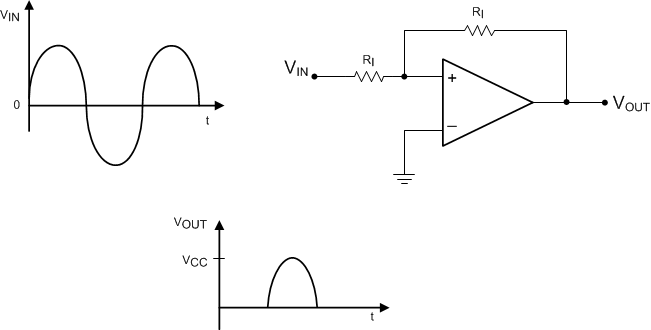 Figure 30. Half-Wave Rectifier With Rail-to-Ground Output Swing Referenced to Ground
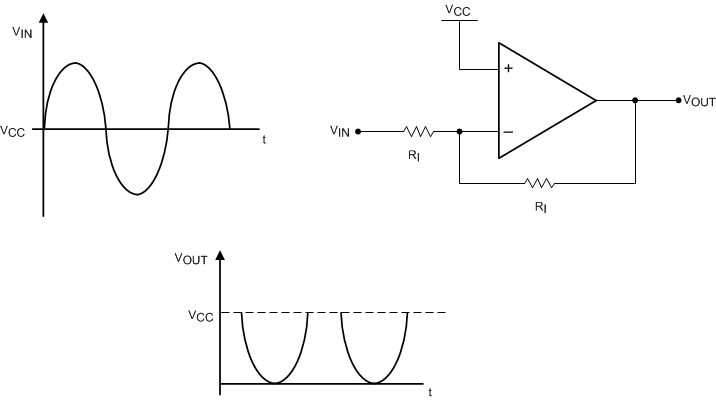 Figure 31. Half-Wave Rectifier With Negative-Going Output Referenced to VCC
8.1.2 Instrumentation Amplifier With Rail-to-Rail Input and Output
Some manufactures make rail-to-rail op amps out of op amps that are otherwise non-rail-to-rail by using a resistive divider on the inputs. The resistors divide the input voltage to get a rail-to-rail input range. The problem with this method is that it also divides the signal, so to get the obtained gain, the amplifier must have a higher closed-loop gain. This raises the noise and drift by the internal gain factor and lowers the input impedance. Any mismatch in these precision resistors reduces the CMRR, as well. The LMV61x is rail-to-rail and therefore doesn’t have these disadvantages.
Using three of the LMV61x amplifiers, an instrumentation amplifier with rail-to-rail inputs and outputs can be made as shown in Figure 32.
In this example, amplifiers on the left side act as buffers to the differential stage. These buffers assure that the input impedance is very high and require no precision matched resistors in the input stage. They also assure that the difference amp is driven from a voltage source. This is necessary to maintain the CMRR set by the matching R1-R2 with R3-R4. The gain is set by the ratio of R2/R1 and R3 must equal R1 and R4 equal R2. With both rail-to-rail input and output ranges, the input and output are only limited by the supply voltages. Remember that even with rail-to-rail outputs, the output can not swing past the supplies so the combined common-mode voltages plus the signal must not be greater that the supplies or limiting occurs.
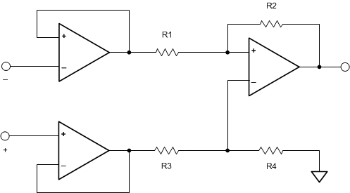 Figure 32. Rail-to-Rail Instrumentation Amplifier
8.2 Typical Applications
8.2.1 High-Side Current Sensing
 Figure 33. High-Side, Current-Sensing Schematic
8.2.1.1 Design Requirements
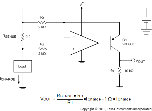
The high-side, current-sensing circuit (Figure 33) is commonly used in a battery charger to monitor charging current to prevent overcharging. A sense resistor RSENSE is connected to the battery directly. This system requires an op amp with rail-to-rail input. The LMV61x are ideal for this application because its common-mode input range goes up to the rail.
8.2.1.1.1 Custom Design With WEBENCH® Tools
Click here to create a custom design using the LMV61x devices with the WEBENCH® Power Designer.
- Start by entering the input voltage (VIN), output voltage (VOUT), and output current (IOUT) requirements.
- Optimize the design for key parameters such as efficiency, footprint, and cost using the optimizer dial.
- Compare the generated design with other possible solutions from Texas Instruments.
The WEBENCH Power Designer provides a customized schematic along with a list of materials with real-time pricing and component availability.
In most cases, these actions are available:
- Run electrical simulations to see important waveforms and circuit performance
- Run thermal simulations to understand board thermal performance
- Export customized schematic and layout into popular CAD formats
- Print PDF reports for the design, and share the design with colleagues
Get more information about WEBENCH tools at www.ti.com/WEBENCH.
8.2.1.2 Detailed Design Procedure
As seen in (Figure 33), the ICHARGE current flowing through sense resistor RSENSE develops a voltage drop equal to VSENSE. The voltage at the negative sense point is now less than the positive sense point by an amount proportional to the VSENSE voltage.
The low-bias currents of the LMV61x cause little voltage drop through R2, so the negative input of the LMV61x amplifier is at essentially the same potential as the negative sense input.
The LMV61x detects this voltage error between its inputs and servo the transistor base to conduct more current through Q1, increasing the voltage drop across R1 until the LMV61x inverting input matches the noninverting input. At this point, the voltage drop across R1 now matches VSENSE.
IG, a current proportional to ICHARGE, flows according to Equation 1.
IG also flows through the gain resistor R3 developing a voltage drop equal to Equation 2.
where
- G = R3 / R1
The other channel of the LMV61x may be used to buffer the voltage across R3 to drive the following stages.
8.2.1.2.1 Application Curve
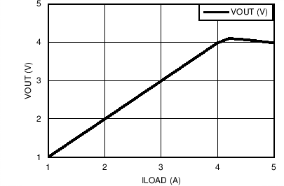 Figure 34. High-Side, Current-Sensing Results

