SNOS534J February 2001 – November 2016 LMV712-N , LMV712-N-Q1
PRODUCTION DATA.
- 1 Features
- 2 Applications
- 3 Description
- 4 Revision History
- 5 Pin Configuration and Functions
- 6 Specifications
- 7 Detailed Description
- 8 Application and Implementation
- 9 Power Supply Recommendations
- 10Layout
- 11Device and Documentation Support
- 12Mechanical, Packaging, and Orderable Information
Package Options
Mechanical Data (Package|Pins)
Thermal pad, mechanical data (Package|Pins)
Orderable Information
1 Features
- Available In Automotive AEC-Q100 Grade 1 Version (LMV712-N Only)
- 5-MHz GBP
- Slew Rate: 5 V/µs
- Low Noise: 20 nV/√Hz
- Supply Current: 1.22 mA/Channel
- VOS< 3 mV Maximum
- Ensured 2.7-V and 5-V Specifications
- Temperature Range: –40°C to 125°C
- Rail-to-Rail Inputs and Outputs
- Unity Gain Stable
- Small Package: 10-Pin DSBGA, 10-Pin WSON, and 10-Pin VSSOP
- 1.5-µA Shutdown ICC
- 2.2-µs Turnon
2 Applications
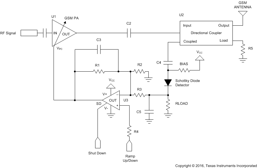
- Power Amplifier Control Loops
- Cellular Phones
- Portable Equipment
- Wireless LAN
- Radio Systems
- Cordless Phones
3 Description
The LMV712-N devices are high-performance BiCMOS operational amplifiers intended for applications requiring rail-to-rail inputs combined with speed and low noise. They offer a bandwidth of
5 MHz and a slew rate of 5 V/µs, and can handle capacitive loads of up to 200 pF without oscillation.
The LMV712-N is ensured to operate from 2.7 V to 5.5 V and offers two independent shutdown pins. This feature allows disabling of each device separately and reduces the supply current to less than 1 µA typical. The output voltage rapidly ramps up smoothly with no glitch as the amplifier comes out of the shutdown mode.
The LMV712-N with the shutdown feature is offered in space-saving 10-pin DSBGA and 10-pin WSON packages. It is also offered in 10-pin VSSOP package. These packages are designed to meet the demands of small size, low power, and low cost required by cellular phones and similar battery-operated portable electronics.
Device Information(1)
| PART NUMBER | PACKAGE | BODY SIZE (NOM) |
|---|---|---|
| LMV712-N | DSBGA (10) | 1.75 mm × 2.25 mm |
| WSON (10) | 3.00 mm × 3.00 mm | |
| LMV712-N, LMV712-N-Q1 |
VSSOP (10) | 3.00 mm × 3.00 mm |
- For all available packages, see the orderable addendum at the end of the data sheet.
Power Amplifier Control Loop
