SNOS032I August   1999  – June 2016 LMV821-N , LMV822-N , LMV822-N-Q1 , LMV824-N , LMV824-N-Q1

PRODUCTION DATA.  

  1. Features
  2. Applications
  3. Description
  4. Revision History
  5. Pin Configuration and Functions
  6. Specifications
    1. 6.1  Absolute Maximum Ratings
    2. 6.2  ESD Ratings
    3. 6.3  Recommended Operating Conditions
    4. 6.4  Thermal Information, 5 Pins
    5. 6.5  Thermal Information, 8 Pins
    6. 6.6  Thermal Information, 14 Pins
    7. 6.7  DC Electrical Characteristics 2.7V
    8. 6.8  DC Electrical Characteristics 2.5V
    9. 6.9  AC Electrical Characteristics 2.7V
    10. 6.10 DC Electrical Characteristics 5V
    11. 6.11 AC Electrical Characteristics 5V
    12. 6.12 Typical Characteristics
  7. Detailed Description
    1. 7.1 Overview
    2. 7.2 Functional Block Diagram
    3. 7.3 Feature Description
    4. 7.4 Device Functional Modes
      1. 7.4.1 Frequency and Phase Response Considerations
      2. 7.4.2 Unity Gain Pulse Response Consideration
      3. 7.4.3 Input Bias Current Consideration
  8. Application and Implementation
    1. 8.1 Application Information
    2. 8.2 Typical Applications
      1. 8.2.1 Telephone-Line Transceiver
        1. 8.2.1.1 Design Requirements
        2. 8.2.1.2 Detailed Design Procedure
      2. 8.2.2 “Simple” Mixer (Amplitude Modulator)
        1. 8.2.2.1 Design Requirements
        2. 8.2.2.2 Detailed Design Procedure
        3. 8.2.2.3 Application Performance Plot
      3. 8.2.3 Tri-Level Voltage Detector
        1. 8.2.3.1 Design Requirements
        2. 8.2.3.2 Detailed Design Procedure
        3. 8.2.3.3 Application Performance Plot
      4. 8.2.4 Dual Amplifier Active Filters (DAAFs)
        1. 8.2.4.1 Design Requirements
        2. 8.2.4.2 Detailed Design Procedure
        3. 8.2.4.3 Application Perfromance Plots
    3. 8.3 Do's and Don'ts
  9. Power Supply Recommendations
  10. 10Layout
    1. 10.1 Layout Guidelines
    2. 10.2 Layout Example
  11. 11Device and Documentation Support
    1. 11.1 Documentation Support
      1. 11.1.1 Related Documentation
    2. 11.2 Receiving Notification of Documentation Updates
    3. 11.3 Community Resources
    4. 11.4 Related Links
    5. 11.5 Trademarks
    6. 11.6 Electrostatic Discharge Caution
    7. 11.7 Glossary
  12. 12Mechanical, Packaging, and Orderable Information

Package Options

Mechanical Data (Package|Pins)
Thermal pad, mechanical data (Package|Pins)
Orderable Information

Pin Configuration and Functions

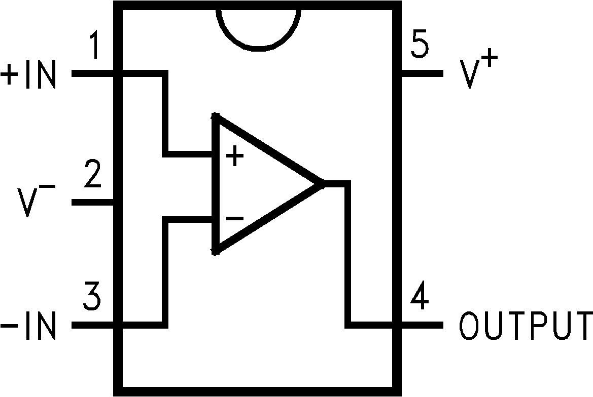
5-Pin SC70-5/SOT23-5
DCK0005A, DBV0005A Packages
Top View
LMV821-N LMV822-N LMV822-N-Q1 LMV824-N LMV824-N-Q1 10012884.png
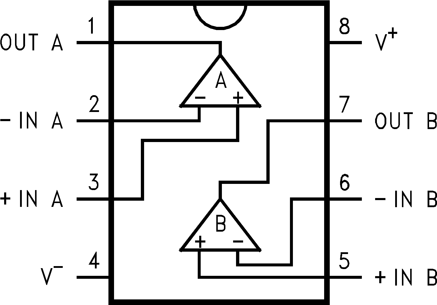
8-Pin SOIC/VSSOP
D0008A, DGK0008A Packages
Top View
LMV821-N LMV822-N LMV822-N-Q1 LMV824-N LMV824-N-Q1 10012863.png
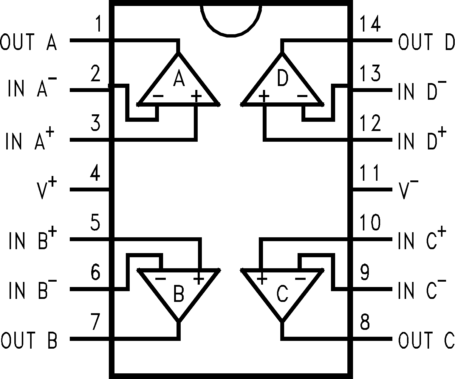
14-Pin SOIC/TSSOP/TVSOP
D0014A, PW0014A, DGV0014A Packages
Top View
LMV821-N LMV822-N LMV822-N-Q1 LMV824-N LMV824-N-Q1 10012885.png

Pin Functions

PIN NAME I/O DESCRIPTION
+IN I Non-Inverting Input
-IN I Inverting Input
OUT O Output
V- P Negative Supply
V+ P Positive Supply