SNOS032I August 1999 – June 2016 LMV821-N , LMV822-N , LMV822-N-Q1 , LMV824-N , LMV824-N-Q1
PRODUCTION DATA.
- 1 Features
- 2 Applications
- 3 Description
- 4 Revision History
- 5 Pin Configuration and Functions
-
6 Specifications
- 6.1 Absolute Maximum Ratings
- 6.2 ESD Ratings
- 6.3 Recommended Operating Conditions
- 6.4 Thermal Information, 5 Pins
- 6.5 Thermal Information, 8 Pins
- 6.6 Thermal Information, 14 Pins
- 6.7 DC Electrical Characteristics 2.7V
- 6.8 DC Electrical Characteristics 2.5V
- 6.9 AC Electrical Characteristics 2.7V
- 6.10 DC Electrical Characteristics 5V
- 6.11 AC Electrical Characteristics 5V
- 6.12 Typical Characteristics
- 7 Detailed Description
- 8 Application and Implementation
- 9 Power Supply Recommendations
- 10Layout
- 11Device and Documentation Support
- 12Mechanical, Packaging, and Orderable Information
Package Options
Mechanical Data (Package|Pins)
Thermal pad, mechanical data (Package|Pins)
Orderable Information
8 Application and Implementation
8.1 Application Information
The LMV82x bring performance and economy to low voltage/low power systems. They provide rail-to-rail output swing into heavy loads and are capable of driving large capacitive loads.
8.2 Typical Applications
8.2.1 Telephone-Line Transceiver
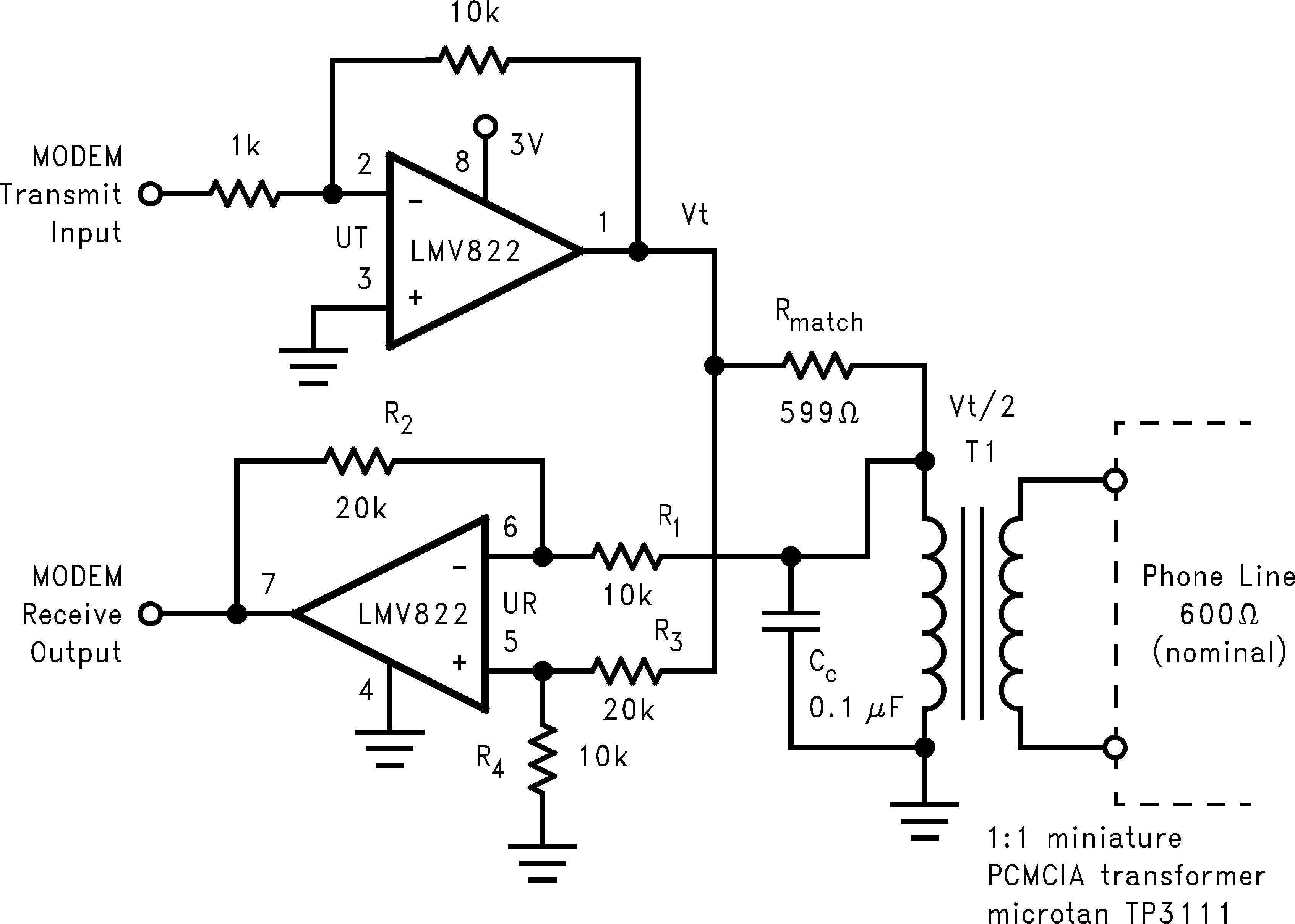 Figure 39. Telephone-Line Transceiver for a PCMCIA Modem Card
8.2.1.1 Design Requirements
The telephone-line transceiver of Figure 39 provides a full-duplexed connection through a PCMCIA, miniature transformer. The differential configuration of receiver portion (UR), cancels reception from the transmitter portion (UT). Note that the input signals for the differential configuration of UR, are the transmit voltage (VT) and VT/2. This is because Rmatch is chosen to match the coupled telephone-line impedance; therefore dividing VT by two (assuming R1 >> Rmatch).
8.2.1.2 Detailed Design Procedure
The differential configuration of UR has its resistors chosen to cancel the VT and VT/2 inputs according to the following equation:

Note that Cc is included for canceling out the inadequacies of the lossy, miniature transformer.
8.2.2 “Simple” Mixer (Amplitude Modulator)
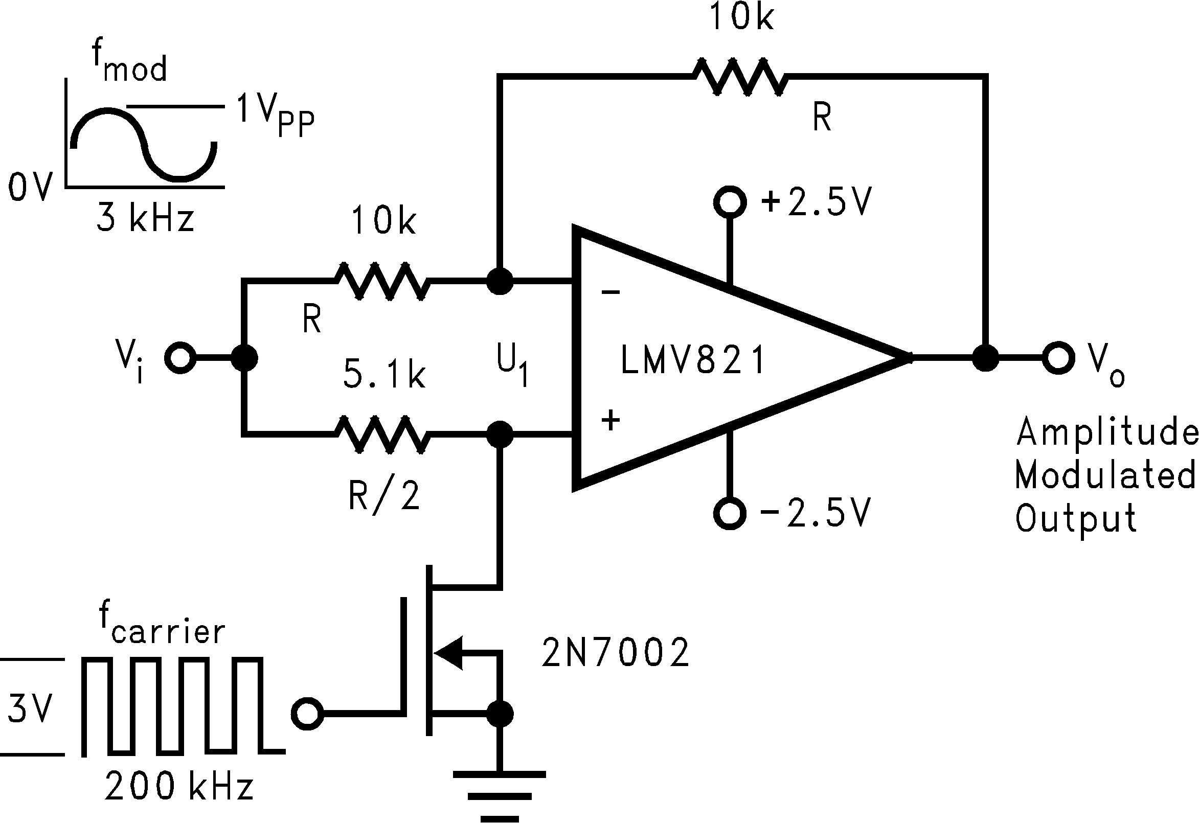 Figure 40. Amplitude Modulator Circuit
8.2.2.1 Design Requirements
The simple mixer can be applied to applications that utilize the Doppler Effect to measure the velocity of an object. The difference frequency is one of its output frequency components. This difference frequency magnitude (/FM-FC/) is the key factor for determining an object's velocity per the Doppler Effect. If a signal is transmitted to a moving object, the reflected frequency will be a different frequency. This difference in transmit and receive frequency is directly proportional to an object's velocity.
8.2.2.2 Detailed Design Procedure
The mixer of Figure 40 is simple and provides a unique form of amplitude modulation. Vi is the modulation frequency (FM), while a +3V square-wave at the gate of Q1, induces a carrier frequency (FC). Q1 switches (toggles) U1 between inverting and non-inverting unity gain configurations. Offsetting a sine wave above ground at Vi results in the oscilloscope photo of Figure 41.
8.2.2.3 Application Performance Plot
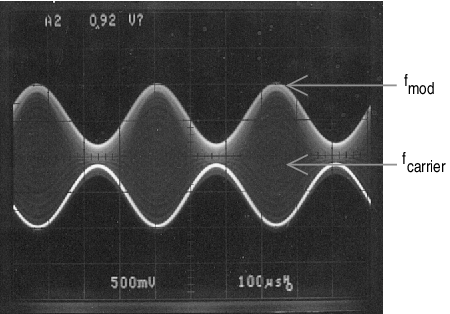 Figure 41. Output signal of Figure 40
8.2.3 Tri-Level Voltage Detector
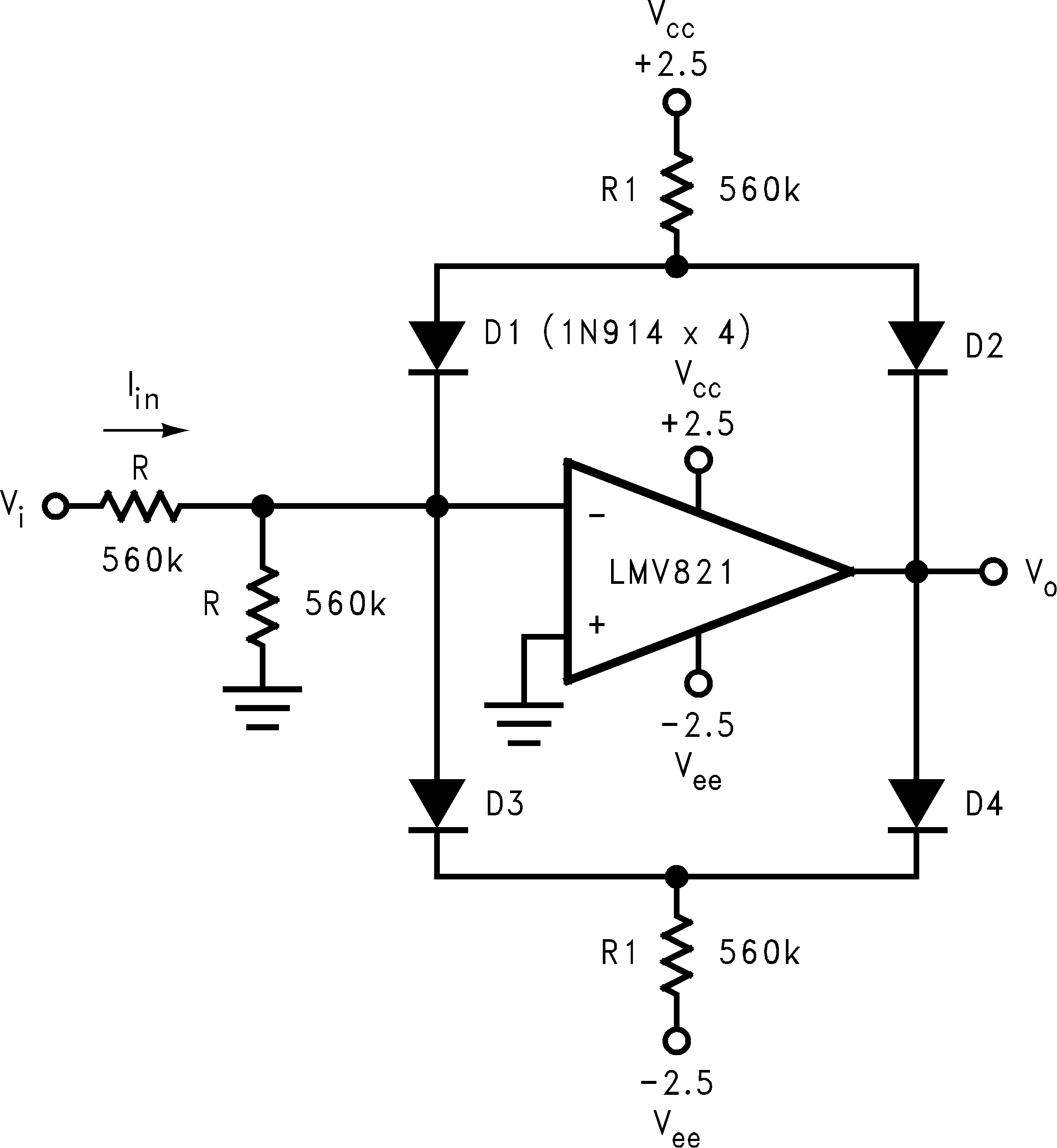 Figure 42. Tri-level Voltage Detector
8.2.3.1 Design Requirements
The tri-level voltage detector of Figure 42 provides a type of window comparator function. It detects three different input voltage ranges: Min-range, Mid-range, and Max-range. The output voltage (VO) is at VCC for the Min-range. VO is clamped at GND for the Mid-range. For the Max-range, VO is at Vee. Figure 43 shows a VO vs. VI oscilloscope photo per the circuit of Figure 42.
Its operation is as follows: VI deviating from GND, causes the diode bridge to absorb IIN to maintain a clamped condition (VO= 0V). Eventually, IIN reaches the bias limit of the diode bridge. When this limit is reached, the clamping effect stops and the op amp responds open loop. The design equation directly preceding Figure 43, shows how to determine the clamping range. The equation solves for the input voltage band on each side GND. The mid-range is twice this voltage band.
8.2.3.2 Detailed Design Procedure

8.2.3.3 Application Performance Plot
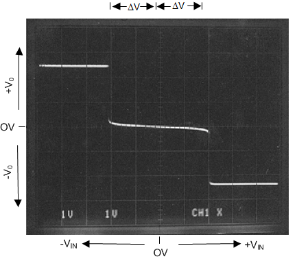 Figure 43. X, Y Oscilloscope Trace showing VOUT vs VIN per the Circuit of Tri-Level Voltage Detector
8.2.4 Dual Amplifier Active Filters (DAAFs)
8.2.4.1 Design Requirements
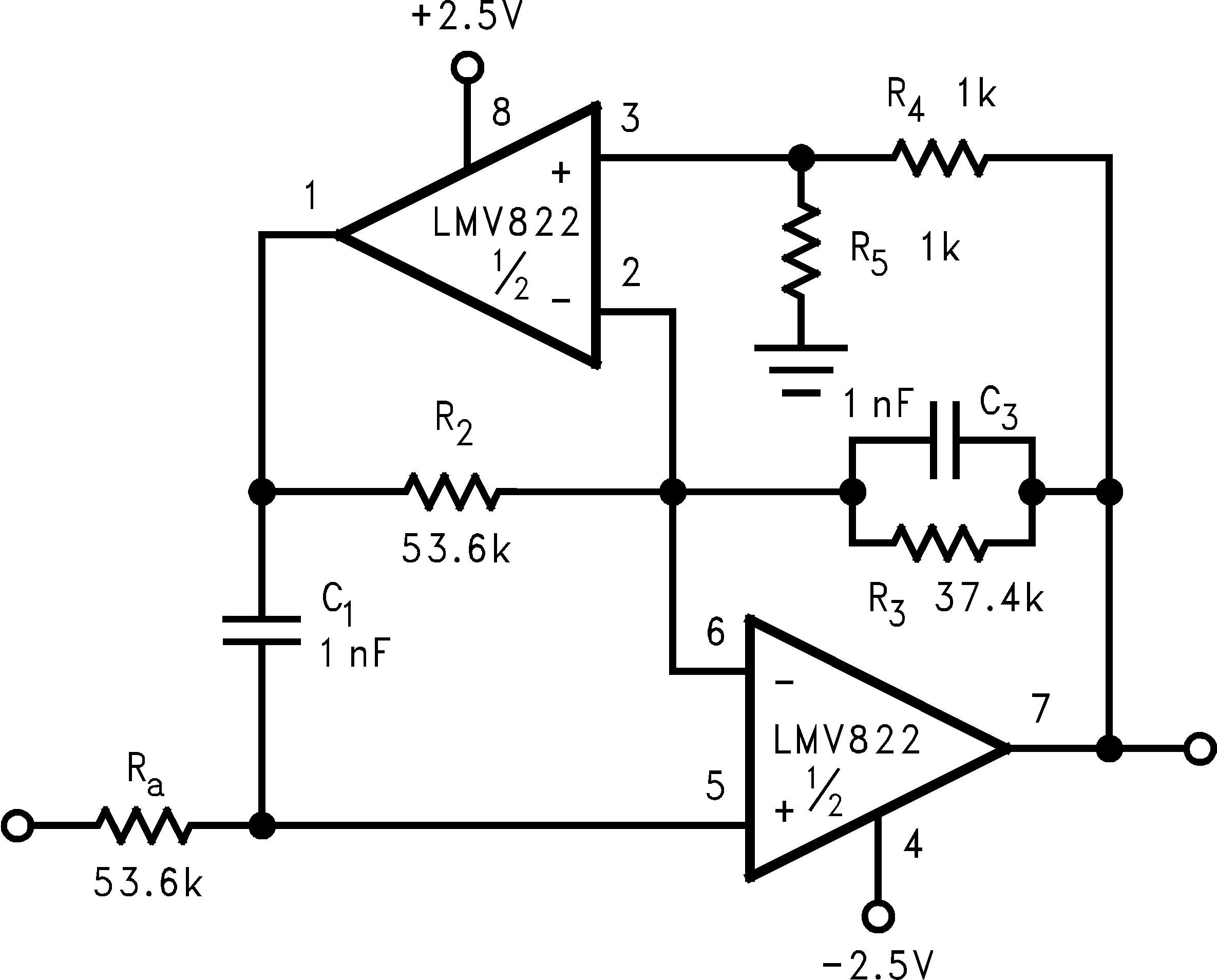
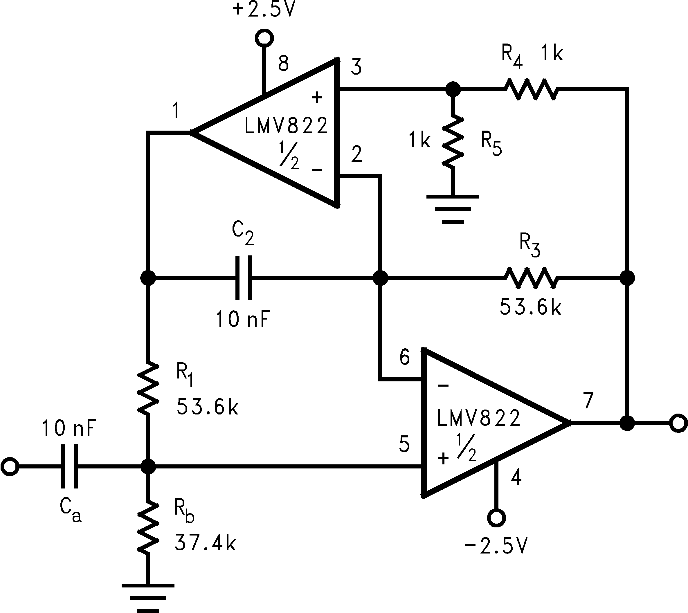
The LMV822/24 bring economy and performance to DAAFs. The low-pass and the high-pass filters of Figure 44 and Figure 45 (respectively), offer one key feature: excellent sensitivity performance. Good sensitivity is when deviations in component values cause relatively small deviations in a filter's parameter such as cutoff frequency (Fc). Single amplifier active filters like the Sallen-Key provide relatively poor sensitivity performance that sometimes cause problems for high production runs; their parameters are much more likely to deviate out of specification than a DAAF would. The DAAFs of Figure 44 and Figure 45 are well suited for high volume production.
8.2.4.2 Detailed Design Procedure
Active filters are also sensitive to an op amp's parameters -Gain and Bandwidth, in particular. The LMV822/24 provide a large gain and wide bandwidth. And DAAFs make excellent use of these feature specifications.
Single Amplifier versions require a large open-loop to closed-loop gain ratio - approximately 50 to 1, at the Fc of the filter response.
In addition to performance, DAAFs are relatively easy to design and implement. The design equations for the low-pass and high-pass DAAFs are shown below. The first two equation calculate the Fc and the circuit Quality Factor (Q) for the LPF (Figure 44). The second two equations calculate the Fc and Q for the HPF (Figure 45).
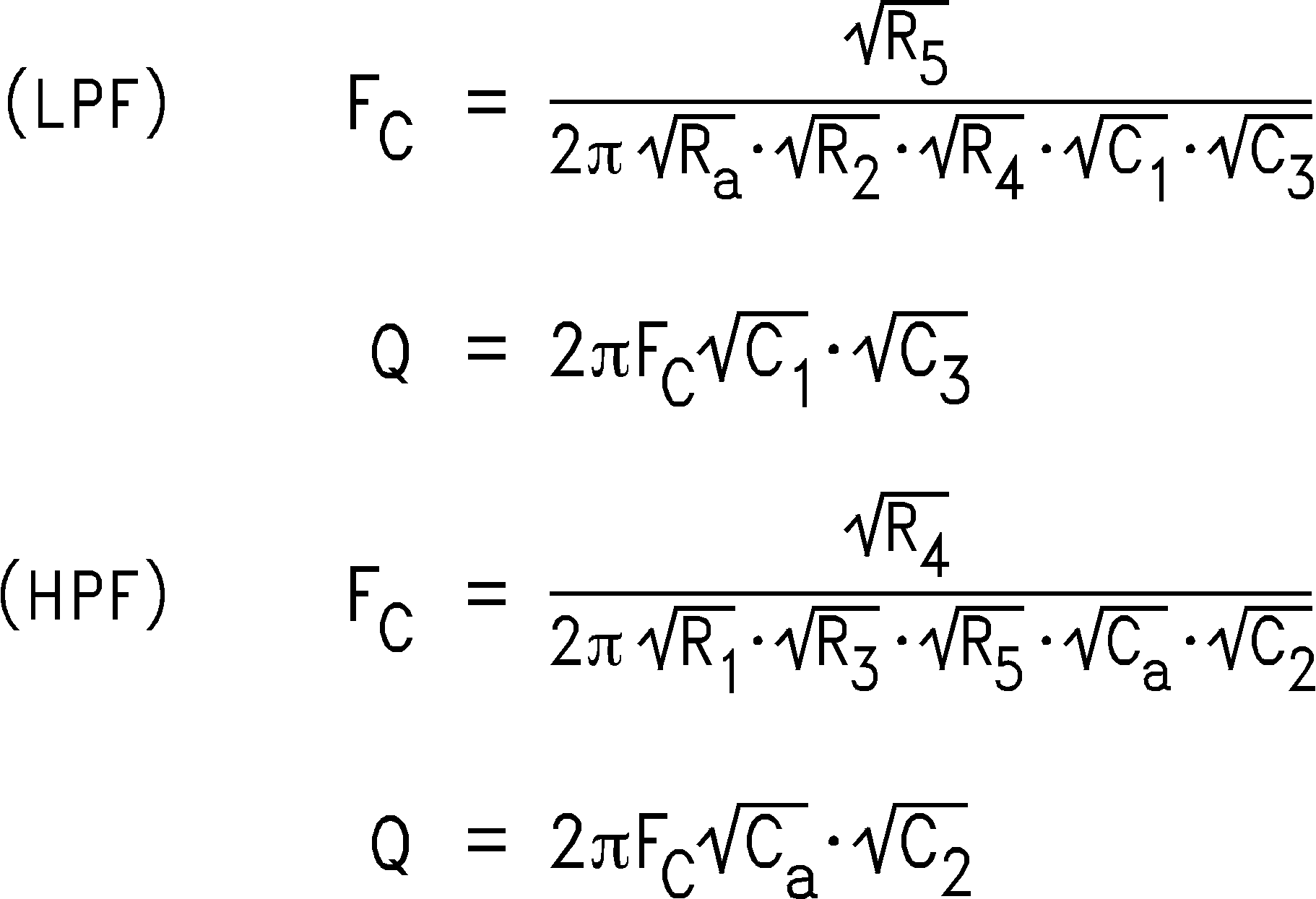
To simplify the design process, certain components are set equal to each other. Refer to Figure 44 and Figure 45. These equal component values help to simplify the design equations as follows:
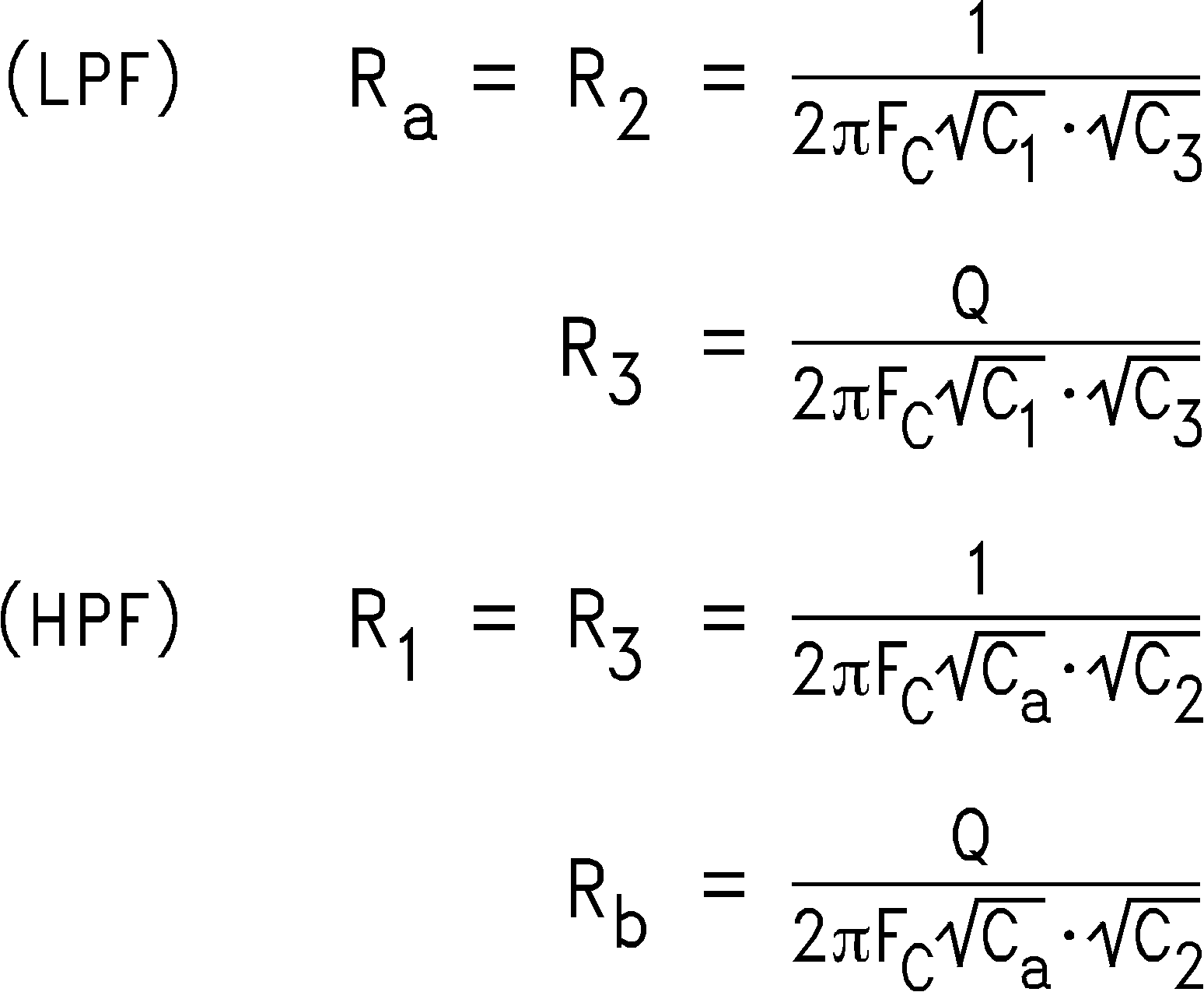
To illustrate the design process/implementation, a 3 kHz, Butterworth response, low-pass filter DAAF (Figure 44) is designed as follows:
1. Choose C1 = C3 = C = 1 nF
2. Choose R4 = R5 = 1 kΩ
3. Calculate Ra and R2 for the desired Fc as follows:
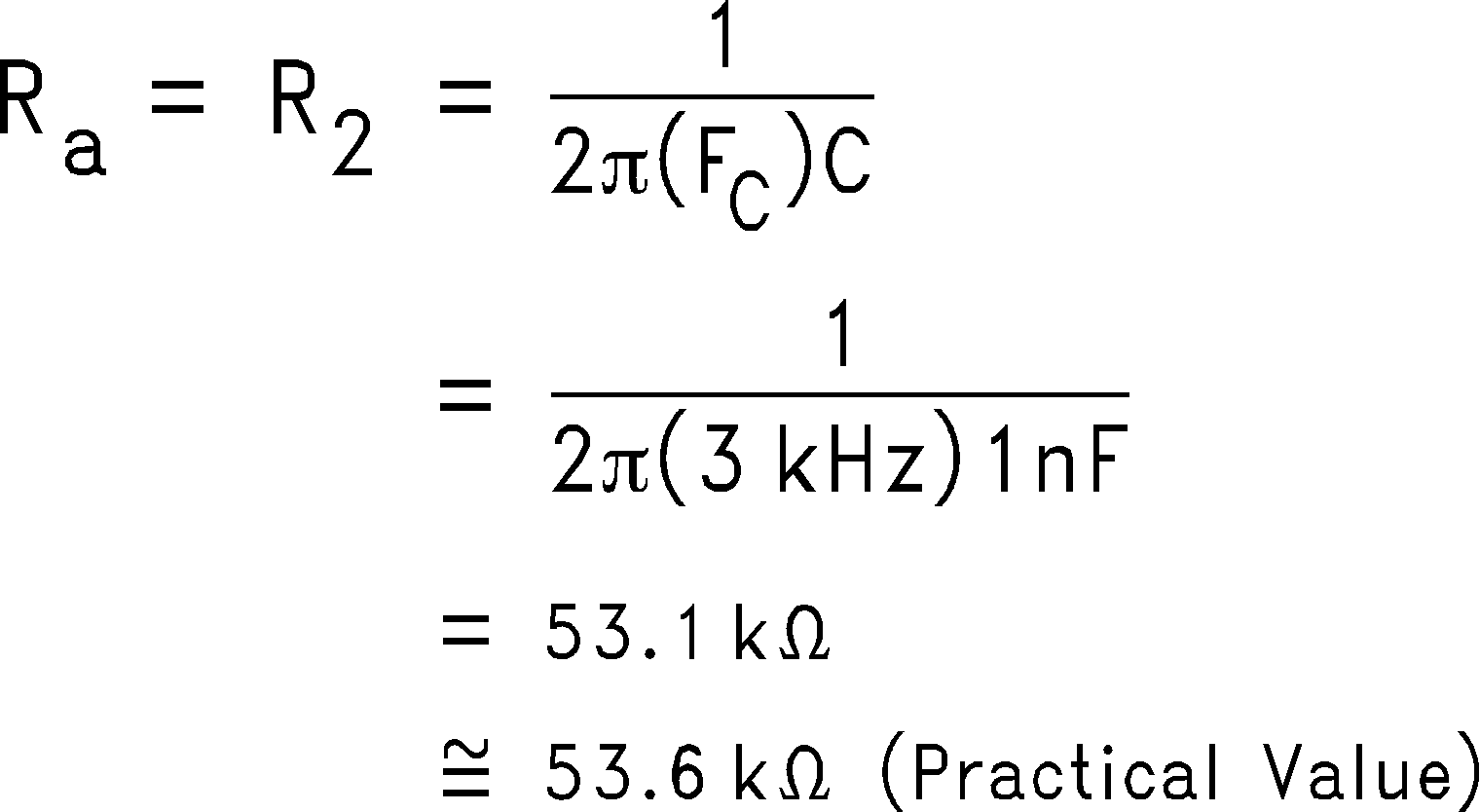
4. Calculate R3 for the desired Q. The desired Q for a Butterworth (Maximally Flat) response is 0.707 (45 degrees into the s-plane). R3 calculates as follows:
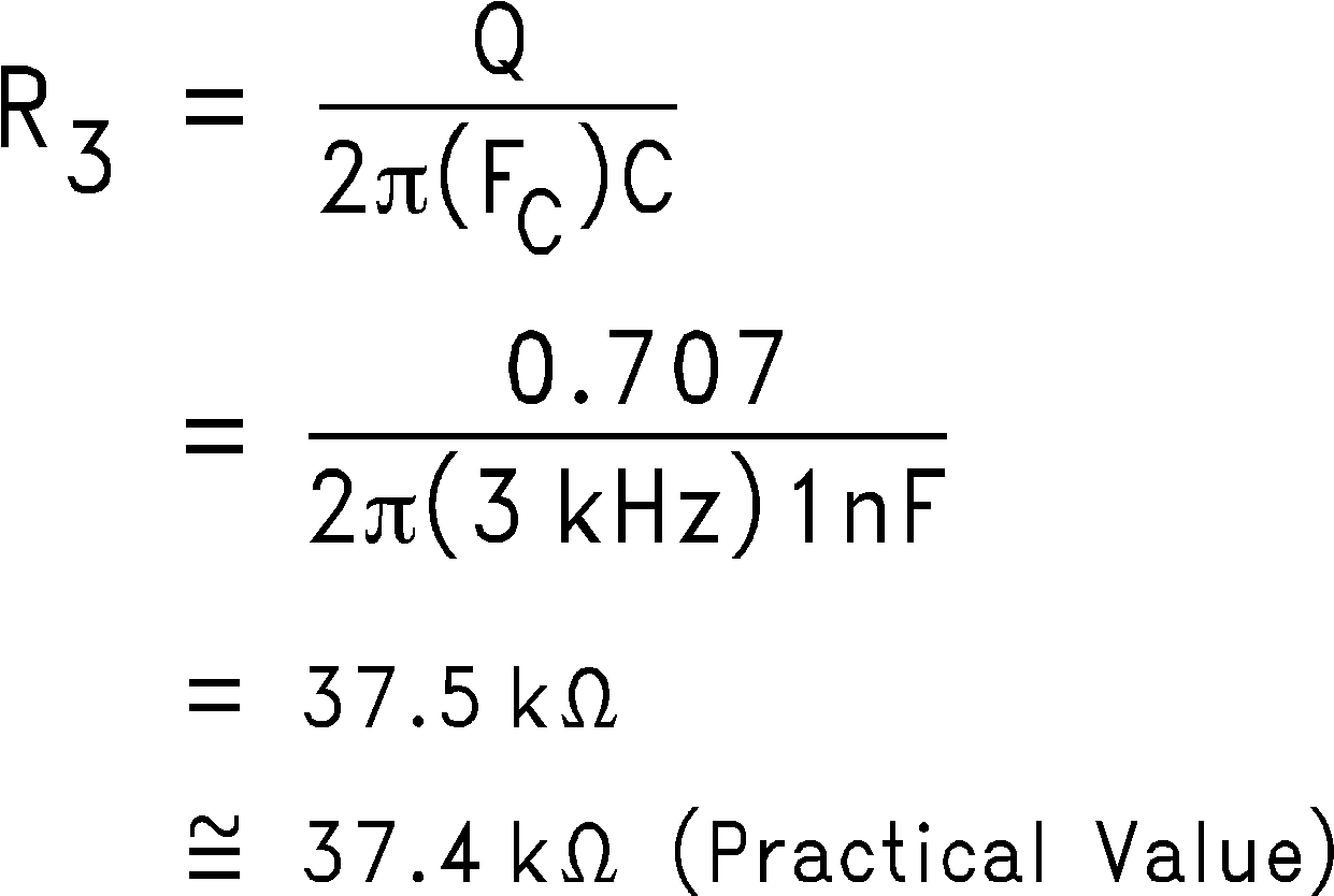
Notice that R3 could also be calculated as 0.707 of Ra or R2.
The circuit was implemented and its cutoff frequency measured. The cutoff frequency measured at 2.92 kHz.
The circuit also showed good repeatability. Ten different LMV822 samples were placed in the circuit. The corresponding change in the cutoff frequency was less than a percent.
8.2.4.3 Application Perfromance Plots
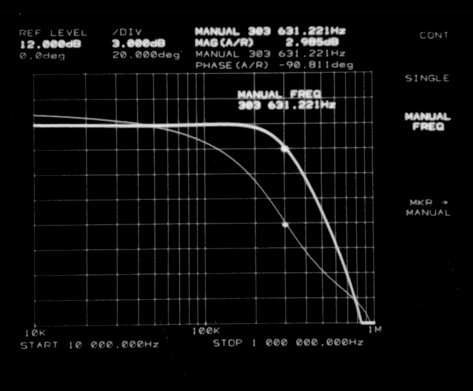
Figure 46 shows an impressive photograph of a network analyzer measurement (HP3577A). The measurement was taken from a 300 kHz version of Figure 44. At 300 kHz, the open-loop to closed-loop gain ratio @ Fc is about 5 to 1. This is 10 times lower than the 50 to 1 “rule of thumb” for Single Amplifier Active Filters.
Table 1 provides sensitivity measurements for a 10 MΩ load condition. The left column shows the passive components for the 3 kHz low-pass DAAF. The third column shows the components for the 300 Hz high-pass DAAF. Their respective sensitivity measurements are shown to the right of each component column. Their values consists of the percent change in cutoff frequency (Fc) divided by the percent change in component value. The lower the sensitivity value, the better the performance.
Each resistor value was changed by about 10 percent, and this measured change was divided into the measured change in Fc. A positive or negative sign in front of the measured value, represents the direction Fc changes relative to components' direction of change. For example, a sensitivity value of negative 1.2, means that for a 1 percent increase in component value, Fc decreases by 1.2 percent.
Note that this information provides insight on how to fine tune the cutoff frequency, if necessary. It should be also noted that R4 and R5 of each circuit also caused variations in the pass band gain. Increasing R4 by ten percent, increased the gain by 0.4 dB, while increasing R5 by ten percent, decreased the gain by 0.4 dB.
Table 1. Component Sensitivity Measurements
| Component (LPF) |
Sensitivity (LPF) |
Component (HPF) |
Sensitivity (HPF) |
|---|---|---|---|
| Ra | -1.2 | Ca | -0.7 |
| C1 | -0.1 | Rb | -1.0 |
| R2 | -1.1 | R1 | +0.1 |
| R3 | +0.7 | C2 | -0.1 |
| C3 | -1.5 | R3 | +0.1 |
| R4 | -0.6 | R4 | -0.1 |
| R5 | +0.6 | R5 | +0.1 |
8.3 Do's and Don'ts
Do properly bypass the power supplies.
Do add series resistence to the oputput when driving capacitive loads, particularly cables, Muxes and ADC inputs.
Do not exceed the input common mode range. The input is not "Rail to Rail" and will limit upper output swing when configured as followers or other low-gain applications. See the Input Common Mode Voltage Range section of the Electrical Table.
Do add series current limiting resistors and external schottky clamp diodes if input voltage is expected to exceed the supplies. Limit the current to 1mA or less (1KΩ per volt).