SNOSAZ6C August 2008 – November 2015 LMV831 , LMV832 , LMV834
PRODUCTION DATA.
- 1 Features
- 2 Applications
- 3 Description
- 4 Revision History
- 5 Pin Configuration and Functions
- 6 Specifications
- 7 Detailed Description
- 8 Application and Implementation
- 9 Power Supply Recommendations
- 10Layout
- 11Device and Documentation Support
- 12Mechanical, Packaging, and Orderable Information
Package Options
Mechanical Data (Package|Pins)
- DCK|5
Thermal pad, mechanical data (Package|Pins)
Orderable Information
7.3.3.2 Cell Phone Call
The effect of electromagnetic interference is demonstrated in a set-up where a cell phone interferes with a pressure sensor application. The application is shown in Figure 49.
This application needs two operational amplifiers and therefore a dual operational amplifier is used. The operational amplifier configured as a buffer and connected at the negative output of the pressure sensor prevents the loading of the bridge by resistor R2. The buffer also prevents the resistors of the sensor from affecting the gain of the following gain stage. The operational amplifiers are placed in a single-supply configuration.
The experiment is performed on two different dual operational amplifiers: a typical standard operational amplifier and the LMV832, EMI-hardened dual operational amplifier. A cell phone is placed on a fixed position a couple of centimeters from the operational amplifiers in the sensor circuit.
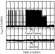
When the cell phone is called, the PCB and wiring connected to the operational amplifiers receive the RF signal. Subsequently, the operational amplifiers detect the RF voltages and currents that end up at their pins. The resulting effect on the output of the second operational amplifier is shown in Figure 45.
 Figure 45. Comparing EMI Robustness
The difference between the two types of dual operational amplifiers is clearly visible. The typical standard dual operational amplifier has an output shift (disturbed signal) larger than 1 V as a result of the RF signal transmitted by the cell phone. The LMV832, EMI-hardened operational amplifier does not show any significant disturbances. This means that the RF signal will not disturb the signal entering the ADC when using the LMV832.