SNOSAT1I October 2006 – October 2017 LMV841 , LMV842 , LMV844
PRODUCTION DATA.
- 1 Features
- 2 Applications
- 3 Description
- 4 Revision History
- 5 Pin Configuration and Functions
- 6 Specifications
- 7 Detailed Description
- 8 Application and Implementation
- 9 Power Supply Recommendations
- 10Layout
- 11Device and Documentation Support
- 12Mechanical, Packaging, and Orderable Information
Package Options
Mechanical Data (Package|Pins)
Thermal pad, mechanical data (Package|Pins)
Orderable Information
8 Application and Implementation
NOTE
Information in the following applications sections is not part of the TI component specification, and TI does not warrant its accuracy or completeness. TI’s customers are responsible for determining suitability of components for their purposes. Customers should validate and test their design implementation to confirm system functionality.
8.1 Application Information
The rail-to-rail input and output of the LMV84x and the wide supply voltage range make these amplifiers ideal to use in numerous applications. Three sample applications, namely the active filter circuit, high-side current sensing, and thermocouple sensor interface, are provided in the Typical Applications section.
8.2 Typical Applications
8.2.1 Active Filter Circuit
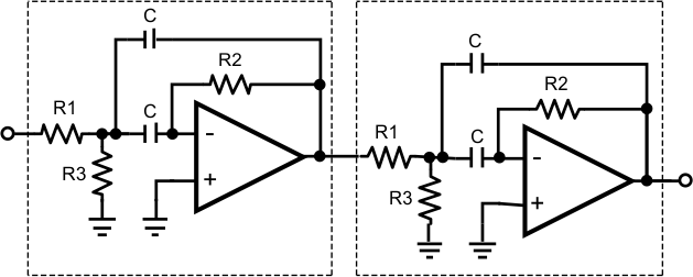 Figure 38. Active Band-Pass Filter Implementation
8.2.1.1 Design Requirements
In this example it is required to design a bandpass filter with band-pass frequency of 10 kHz, and a center frequence of approximately 10% from the total frequence of the filter. This is achieved by cascading two band-pass filters, A and B, with slightly different center frequencies.
8.2.1.2 Detailed Design Procedure
The center frequency of the separate band-pass filters A, and B can be calculated by Equation 16:

where
- C = 33 nF
- R1 = 2 KΩ
- R2 = 6.2 KΩ
- and R3 = 45 Ω
This gives Equation 17 for filter A:

and Equation 18 for filter B with C = 27nF:

Bandwidth can be calculated by Equation 19:

For filter A, this gives Equation 20:

and Equation 21 for filter B:

8.2.1.3 Application Curve
The responses of filter A and filter B are shown as the thin lines in Figure 39; the response of the combined filter is shown as the thick line. Shifting the center frequencies of the separate filters farther apart, results in a wider band; however, positioning the center frequencies too far apart results in a less flat gain within the band. For wider bands more band-pass filters can be cascaded.
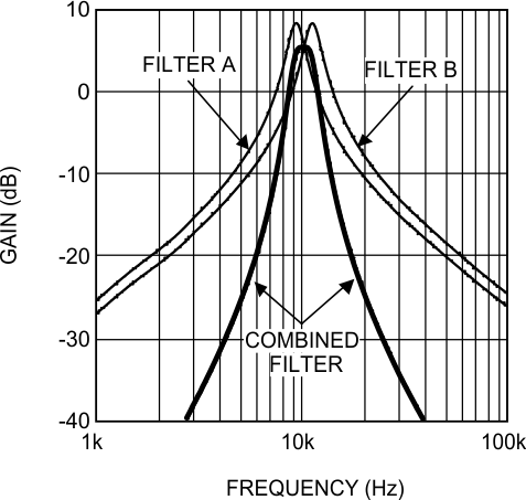 Figure 39. Active Band-Pass Filter Curve
NOTE
Use the WEBENCH internet tools at www.ti.com for your filter application.
8.2.2 High-Side, Current-Sensing Circuit
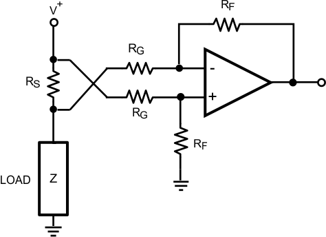 Figure 40. High-Side, Current-Sensing Circuit
8.2.2.1 Design Requirements
In this example, it is desired to measure a current between 0 A and 2 A using a sense resistor of 100 mΩ, and convert it to an output voltage of 0 to 5 V. A current of 2 A flowing through the load and the sense resistor results in a voltage of 200 mV across the sense resistor. The op amp amplifies this 200 mV to fit the current range to the output voltage range.
8.2.2.2 Detailed Design Procedure
To measure current at a point in a circuit, a sense resistor is placed in series with the load, as shown in Figure 40. The current flowing through this sense resistor results in a voltage drop, that is amplified by the op amp. The rail-to-rail input and the low VOS features make the LMV84x ideal op amps for high-side, current-sensing applications.
The input and the output relation of the circuit is given by Equation 22:
For a load current of 2 A and an output voltage of 5 V the gain would be VOUT / VSENSE = 25.
If the feedback resistor, RF, is 100 kΩ, then the value for RG is 4 kΩ. The tolerance of the resistors has to be low to obtain a good common-mode rejection.
8.2.3 Thermocouple Sensor Signal Amplification
Figure 41 is a typical example for a thermocouple amplifier application using an LMV841, LMV842, or LMV844. A thermocouple senses a temperature and converts it into a voltage. This signal is then amplified by the LMV841, LMV842, or LMV844. An ADC can then convert the amplified signal to a digital signal. For further processing the digital signal can be processed by a microprocessor, and can be used to display or log the temperature, or the temperature data can be used in a fabrication process.
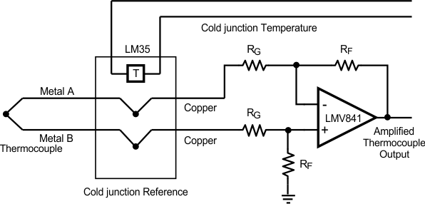 Figure 41. Thermocouple Sensor Interface
8.2.3.1 Design Requirements
In this example it is desired to measure temperature in the range of 0°C to 500°C with a resolution of 0.5°C using a K-type thermocouple sensor. The power supply for both the LMV84x and the ADC is
3.3 V.
8.2.3.2 Detailed Design Procedure
A thermocouple is a junction of two different metals. These metals produce a small voltage that increases with temperature. A K-type thermocouple is a very common temperature sensor made of a junction between nickel-chromium and nickel-aluminum. There are several reasons for using the K-type thermocouple. These include temperature range, the linearity, the sensitivity, and the cost.
A K-type thermocouple has a wide temperature range. The range of this thermocouple is from approximately −200°C to approximately 1200°C, as can be seen in Figure 42. This covers the generally used temperature ranges.
Over the main part of the range the behavior is linear. This is important for converting the analog signal to a digital signal. The K-type thermocouple has good sensitivity when compared to many other types; the sensitivity is 41 µV/°C. Lower sensitivity requires more gain and makes the application more sensitive to noise. In addition, a K-type thermocouple is not expensive, many other thermocouples consist of more expensive materials or are more difficult to produce.
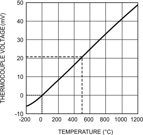 Figure 42. K-Type Thermocouple Response
The temperature range of 0°C to 500°C results in a voltage range from 0 mV to 20.6 mV produced by the thermocouple. This is shown in Figure 42.
To obtain the best accuracy the full ADC range of 0 to 3.3 V is used and the gain needed for this full range can be calculated Equation 23:
If RG is 2 kΩ, then the value for RF can be calculated with this gain of 160. Because AV = RF / RG, RF can be calculated in Equation 24:
To achieve a resolution of 0.5°C a step smaller than the minimum resolution is needed. This means that at least 1000 steps are necessary (500°C/0.5°C). A 10-bit ADC would be sufficient as this gives 1024 steps. A 10-bit ADC such as the two channel 10-bit ADC102S021 would be a good choice.
At the point where the thermocouple wires are connected to the circuit on the PCB unwanted parasitic thermocouple is formed, introducing error in the measurements of the actual thermocouple sensor.
Using an isothermal block as a reference will compensate for this additional thermocouple effect. An isothermal block is a good heat conductor. This means that the two thermocouple connections both have the same temperature. The temperature of the isothermal block can be measured, and thereby the temperature of the thermocouple connections. This is usually called the cold junction reference temperature. In the example, an LM35 is used to measure this temperature. This semiconductor temperature sensor can accurately measure temperatures from −55°C to 150°C.
The ADC in this example also coverts the signal from the LM35 to a digital signal, hence, the microprocessor can compensate for the amplified thermocouple signal of the unwanted thermocouple junction at the connector.