SNAS866A December   2023  – September 2024 LMX1214

PRODUCTION DATA  

  1.   1
  2. Features
  3. Applications
  4. Description
  5. Pin Configuration and Functions
  6. Specifications
    1. 5.1 Absolute Maximum Ratings
    2. 5.2 ESD Ratings
    3. 5.3 Recommended Operating Conditions
    4. 5.4 Thermal Information
    5. 5.5 Electrical Characteristics
    6. 5.6 Timing Requirements
    7. 5.7 Timing Diagram
    8. 5.8 Typical Characteristics
  7. Detailed Description
    1. 6.1 Overview
      1. 6.1.1 Range of Dividers
    2. 6.2 Functional Block Diagram
    3. 6.3 Feature Description
      1. 6.3.1 Power-On Reset
      2. 6.3.2 Temperature Sensor
      3. 6.3.3 Clock Outputs
        1. 6.3.3.1 Clock Output Buffers
        2. 6.3.3.2 Clock MUX
        3. 6.3.3.3 Clock Divider
      4. 6.3.4 AUXCLK Output
        1. 6.3.4.1 AUXCLKOUT Output Format
        2. 6.3.4.2 AUXCLK_DIV_PRE and AUXCLK_DIV Dividers
      5. 6.3.5 SYNC Input Pins
        1. 6.3.5.1 SYNC Pins Common-Mode Voltage
        2. 6.3.5.2 Windowing Feature
    4. 6.4 Device Functional Modes Configurations
      1. 6.4.1 Pin Mode Control
  8. Register Map
    1. 7.1 Device Registers
  9. Application and Implementation
    1. 8.1 Application Information
      1. 8.1.1 SYNC Input Configuration
      2. 8.1.2 Treatment of Unused Pins
      3. 8.1.3 Current Consumption
    2. 8.2 Typical Application
      1. 8.2.1 Design Requirements
      2. 8.2.2 Detailed Design Procedure
      3. 8.2.3 Application Plots
    3. 8.3 Power Supply Recommendations
    4. 8.4 Layout
      1. 8.4.1 Layout Guidelines
      2. 8.4.2 Layout Example
  10. Device and Documentation Support
    1. 9.1 Device Support
    2. 9.2 Documentation Support
      1. 9.2.1 Related Documentation
    3. 9.3 Receiving Notification of Documentation Updates
    4. 9.4 Support Resources
    5. 9.5 Trademarks
    6. 9.6 Electrostatic Discharge Caution
    7. 9.7 Glossary
  11. 10Revision History
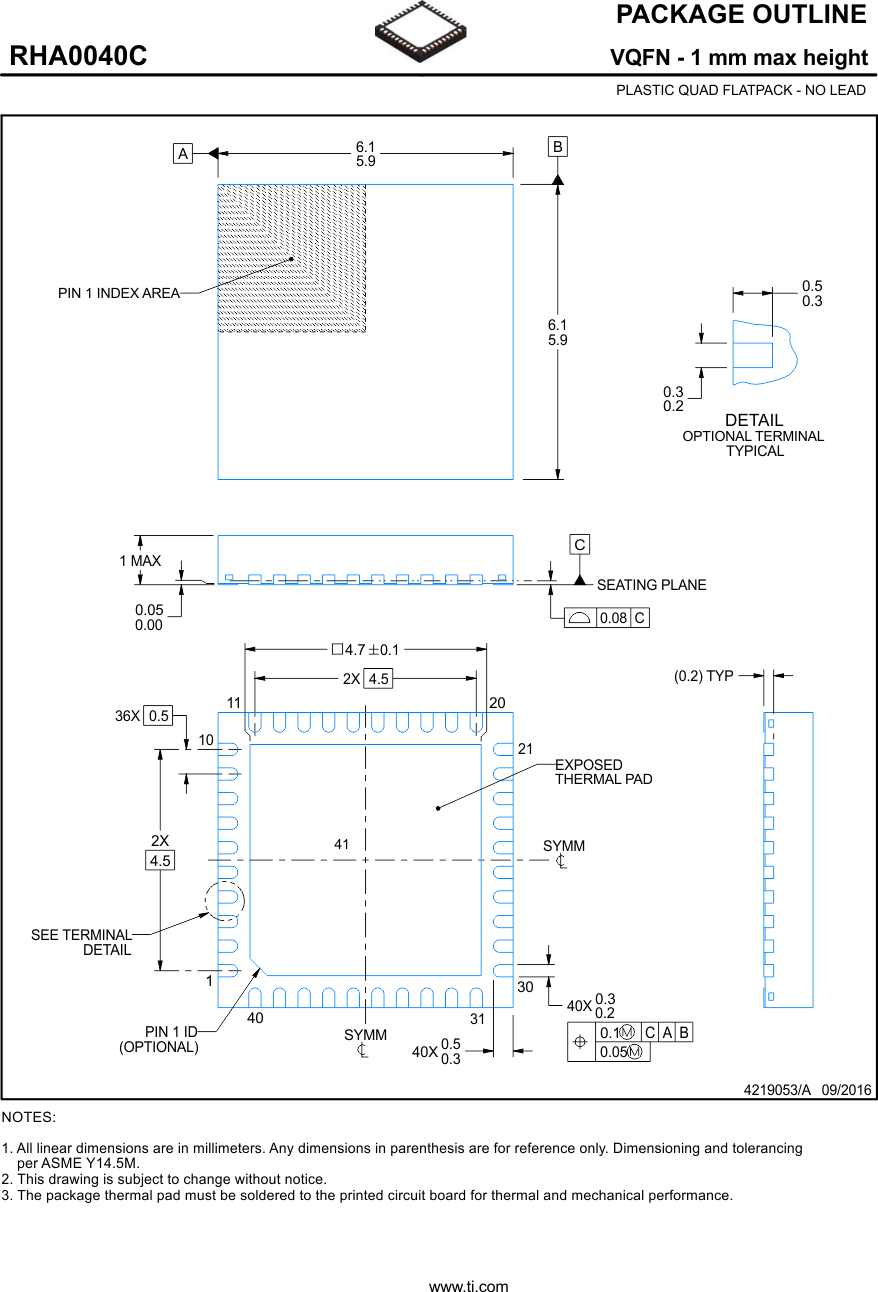
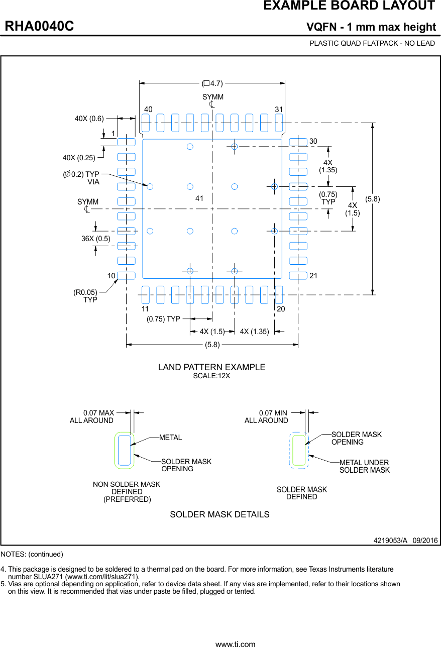
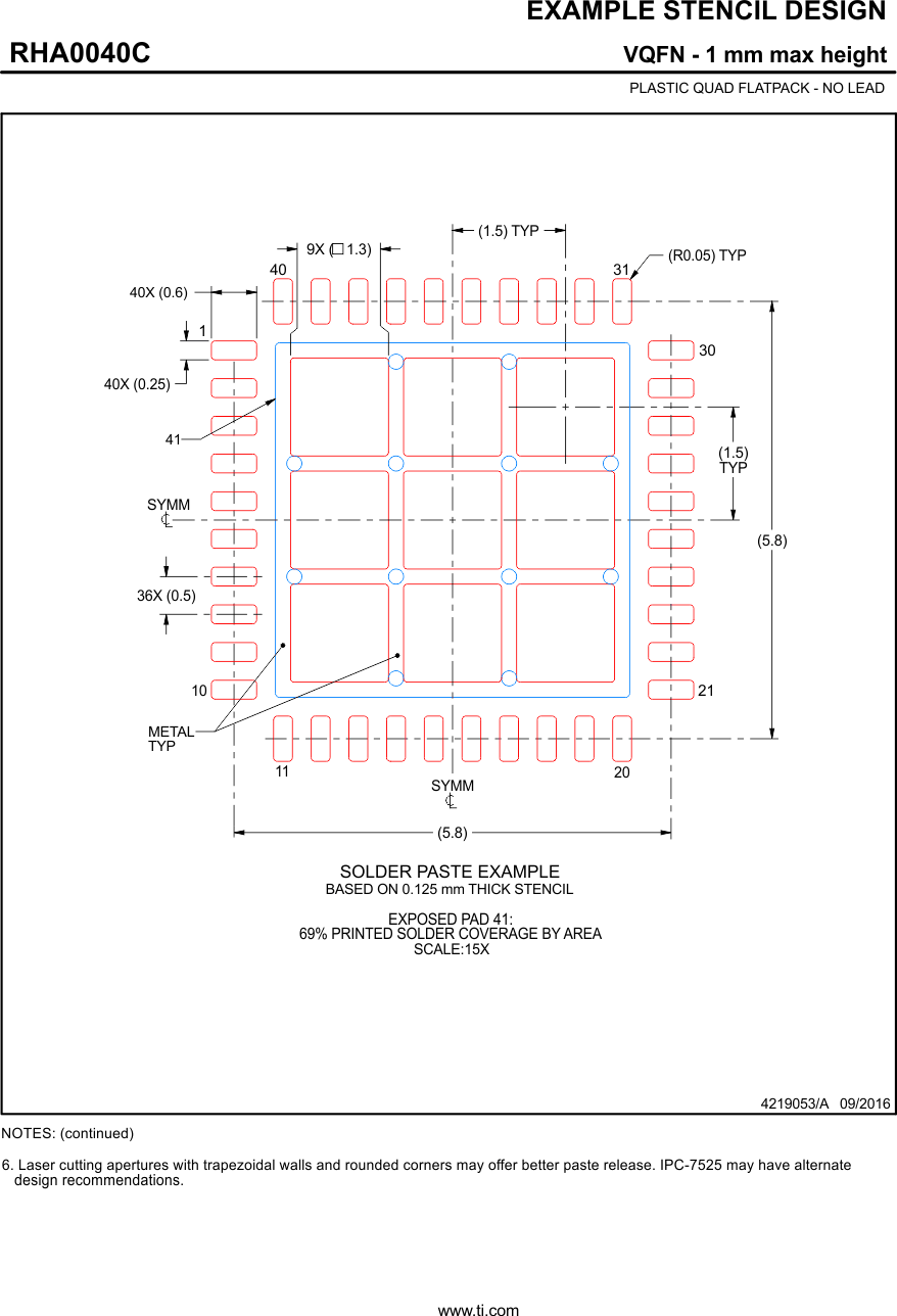
  12. 11Mechanical, Packaging, and Orderable Information
    1. 11.1 Tape and Reel Information

Package Options

Mechanical Data (Package|Pins)
Thermal pad, mechanical data (Package|Pins)
Orderable Information

Mechanical, Packaging, and Orderable Information

The following pages include mechanical, packaging, and orderable information. This information is the most current data available for the designated devices. This data is subject to change without notice and revision of this document. For browser-based versions of this data sheet, refer to the left-hand navigation.


LMX1214

LMX1214

LMX1214