SNAS601G August 2012 – September 2014 LMX2581
PRODUCTION DATA.
- 1 Features
- 2 Applications
- 3 Description
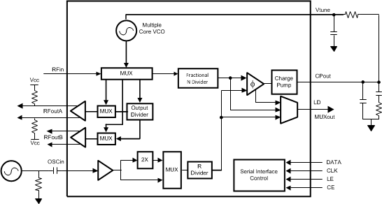
- 4 Simplified Schematic
- 5 Revision History
- 6 Pin Configuration and Functions
- 7 Specifications
-
8 Detailed Description
- 8.1 Overview
- 8.2 Functional Block Diagram
- 8.3
Feature Description
- 8.3.1 Typical Performance Characteristics
- 8.3.2 Impact of Temperature on VCO Phase Noise
- 8.3.3 OSCin INPUT and OSCin Doubler
- 8.3.4 R Divider
- 8.3.5 PLL N Divider And Fractional Circuitry
- 8.3.6 PLL Phase Detector and Charge Pump
- 8.3.7 External Loop Filter
- 8.3.8 Low Noise, Fully Integrated VCO
- 8.3.9 Programmable VCO Divider
- 8.3.10 0-Delay Mode
- 8.3.11 Programmable RF Output Buffers
- 8.3.12 Fastlock
- 8.3.13 Lock Detect
- 8.3.14 Part ID and Register Readback
- 8.3.15 Optimization of Spurs
- 8.4 Device Functional Modes
- 8.5 Programming
- 8.6
Register Maps
- 8.6.1
Programming Word Descriptions
- 8.6.1.1 Register R15
- 8.6.1.2 Register R13
- 8.6.1.3 Registers R10, R9, and R8
- 8.6.1.4 Register R7
- 8.6.1.5 Register R6
- 8.6.1.6
Register R5
- 8.6.1.6.1 OUT_LDEN — Mute Outputs Based on Lock Detect
- 8.6.1.6.2 OSC_FREQ[2:0] — OSCin Frequency for VCO Calibration
- 8.6.1.6.3 BUFEN_DIS - Disable for the BUFEN Pin
- 8.6.1.6.4 VCO_SEL_MODE — Method of Selecting Internal VCO Core
- 8.6.1.6.5 OUTB_MUX — Mux for RFoutB
- 8.6.1.6.6 OUTA_MUX — Mux for RFoutA
- 8.6.1.6.7 0_DLY - Zero Delay Mode
- 8.6.1.6.8 MODE[1:0] — Operating Mode
- 8.6.1.6.9 PWDN_MODE - Powerdown Mode
- 8.6.1.6.10 RESET - Register Reset
- 8.6.1.7 Register R4
- 8.6.1.8 Register R3
- 8.6.1.9 Register R2
- 8.6.1.10 Register R1
- 8.6.1.11 Register R0
- 8.6.1
Programming Word Descriptions
- 9 Application and Implementation
- 10Power Supply Recommendations
- 11Layout
- 12Device and Documentation Support
- 13Mechanical, Packaging, and Orderable Information
Package Options
Mechanical Data (Package|Pins)
- RTV|32
Thermal pad, mechanical data (Package|Pins)
- RTV|32
Orderable Information
1 Features
- Output Frequency from 50 to 3760 MHz
- Input Clock Frequency up to 900 MHz
- Phase Detector Frequency up to 200 MHz
- Supports Fractional and Integer Modes
- –229 dBc/Hz Normalized PLL Phase Noise
- –120.8 dBc/Hz Normalized PLL 1/f Noise
- –137 dBc/Hz VCO Phase Noise @ 1 MHz offset for a 2.5 GHz Carrier
- 100 fs RMS Jitter in Integer Mode
- Programmable Fractional Modulator Order
- Programmable Fractional Denominator
- Programmable Output Power up to +12 dBm
- Programmable 32 Level Charge Pump Current
- Programmable Option to Use an External VCO
- Digital Lock Detect
- 3-Wire Serial Interface and Readback
- Single Supply Voltage from 3.15 V to 3.45 V
- Supports Logic Levels down to 1.6 V
2 Applications
- Wireless Infrastructure (UMTS, LTE, WiMax, Multi-Standard Base Stations)
- Broadband Wireless
- Test and Measurement
- Clock Generation
3 Description
The LMX2581 is a low noise wideband frequency synthesizer that integrates a delta-sigma fractional N PLL, multiple core VCO, programmable output divider, and two differential output buffers. The VCO frequency range is from 1880 to 3760 MHz and can be sent directly to the output buffers or divided down by even values from 2 to 38. Each buffer is capable of output power from -3 to +12 dBm at 2700 MHz. Integrated low noise LDOs are used for superior noise immunity and consistent performance.
This synthesizer is a highly programmable device and it enables the user to optimize its performance. In fractional mode, the denominator and the modulator order are programmable and can be configured with dithering as well. The user also has the ability to directly specify a VCO core or entirely bypass the internal VCO. Finally, many convenient features are included such as power down, Fastlock, auto mute, and lock detection. All registers can be programmed through a simple 3 wire interface and a read back feature is also available.
The LMX2581 operates on a single 3.3 V supply and comes in a 32 pin 5.0 mm × 5.0 mm WQFN package.
Device Information(1)
| PART NUMBER | PACKAGE | BODY SIZE (NOM) |
|---|---|---|
| LMX2581 | WQFN (32) | 5.00 mm × 5.00 mm |
- For all available packages, see the orderable addendum at the end of the datasheet.
4 Simplified Schematic