SNAS783C
June 2020 – February 2021
LMX2820
PRODUCTION DATA
1
Features
2
Applications
3
Description
4
Revision History
5
Pin Configuration and Functions
6
Specifications
6.1
Absolute Maximum Ratings
6.2
ESD Ratings
6.3
Recommended Operating Conditions
6.4
Thermal Information
6.5
Electrical Characteristics
6.6
Timing Requirements
6.7
Typical Characteristics
7
Detailed Description
7.1
Overview
7.2
Functional Block Diagram
7.3
Feature Description
7.3.1
Reference Oscillator Input
7.3.2
Input Path
7.3.2.1
Input Path Doubler (OSC_2X)
7.3.2.2
Pre-R Divider (PLL_R_PRE)
7.3.2.3
Programmable Input Multiplier (MULT)
7.3.2.4
R Divider (PLL_R)
7.3.3
PLL Phase Detector and Charge Pump
7.3.4
N Divider and Fractional Circuitry
7.3.4.1
Integer N Divide Portion (PLL_N)
7.3.4.2
Fractional N Divide Portion (PLL_NUM and PLL_DEN)
7.3.4.3
Modulator Order (MASH_ORDER)
7.3.5
LD Pin Lock Detect
7.3.6
MUXOUT Pin and Readback
7.3.7
Internal VCO
7.3.7.1
VCO Calibration
7.3.7.1.1
Determining the VCO Gain and Ranges
7.3.8
Channel Divider
7.3.9
Output Frequency Doubler
7.3.10
Output Buffer
7.3.11
Power-Down Modes
7.3.12
Phase Synchronization for Multiple Devices
7.3.12.1
SYNC Categories
7.3.12.2
Phase Adjust
7.3.12.2.1
Using MASH_SEED to Create a Phase Shift
7.3.12.2.2
Static vs. Dynamic Phase Adjust
7.3.12.2.3
Fine Adjustments to Phase Adjust
7.3.13
SYSREF
7.3.14
Fast VCO Calibration
7.3.15
Double Buffering (Shadow Registers)
7.3.16
Output Mute Pin and Ping Pong Approaches
7.4
Device Functional Modes
7.4.1
External VCO Mode
7.4.2
External Feedback Input Pins
7.4.2.1
PFDIN External Feedback Mode
7.4.2.2
RFIN External Feedback Mode
8
Application and Implementation
8.1
Application Information
8.1.1
Treatment of Unused Pins
8.1.2
External Loop Filter
8.1.3
Using Instant Calibration
8.2
Typical Application
8.2.1
Design Requirements
8.2.2
Detailed Design Procedure
8.2.3
Application Curves
8.3
Initialization and Power-on Sequencing
9
Power Supply Recommendations
10
Layout
10.1
Layout Guidelines
10.2
Layout Example
11
Device and Documentation Support
11.1
Receiving Notification of Documentation Updates
11.2
Support Resources
11.3
Trademarks
11.4
Electrostatic Discharge Caution
11.5
Glossary
12
Mechanical, Packaging, and Orderable Information
Package Options
Mechanical Data (Package|Pins)
RTC|48
MPQF140D
Thermal pad, mechanical data (Package|Pins)
RTC|48
QFND642
Orderable Information
snas783c_oa
snas783c_pm
7.3.12.1
SYNC Categories
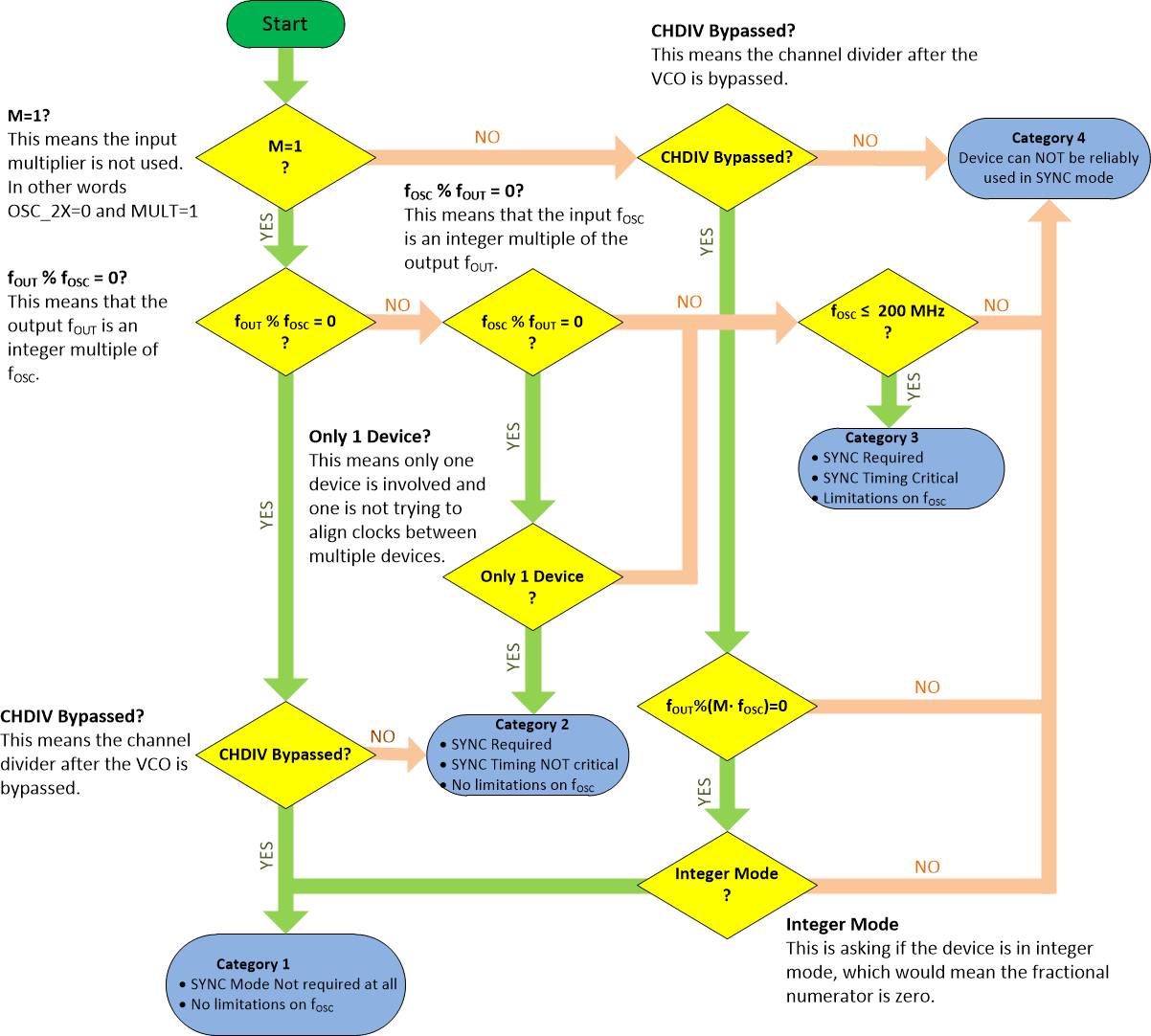
Figure 7-3
Synchronization Flowchart