SNAS783C June 2020 – February 2021 LMX2820
PRODUCTION DATA
- 1 Features
- 2 Applications
- 3 Description
- 4 Revision History
- 5 Pin Configuration and Functions
- 6 Specifications
-
7 Detailed Description
- 7.1 Overview
- 7.2 Functional Block Diagram
- 7.3
Feature Description
- 7.3.1 Reference Oscillator Input
- 7.3.2 Input Path
- 7.3.3 PLL Phase Detector and Charge Pump
- 7.3.4 N Divider and Fractional Circuitry
- 7.3.5 LD Pin Lock Detect
- 7.3.6 MUXOUT Pin and Readback
- 7.3.7 Internal VCO
- 7.3.8 Channel Divider
- 7.3.9 Output Frequency Doubler
- 7.3.10 Output Buffer
- 7.3.11 Power-Down Modes
- 7.3.12 Phase Synchronization for Multiple Devices
- 7.3.13 SYSREF
- 7.3.14 Fast VCO Calibration
- 7.3.15 Double Buffering (Shadow Registers)
- 7.3.16 Output Mute Pin and Ping Pong Approaches
- 7.4 Device Functional Modes
- 8 Application and Implementation
- 9 Power Supply Recommendations
- 10Layout
- 11Device and Documentation Support
- 12Mechanical, Packaging, and Orderable Information
Package Options
Mechanical Data (Package|Pins)
- RTC|48
Thermal pad, mechanical data (Package|Pins)
- RTC|48
Orderable Information
7.4.2.1 PFDIN External Feedback Mode
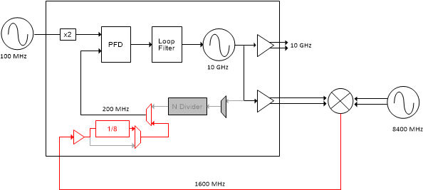
The PFDIN pin allows the VCO frequency to be downconverted externally with a mixer in order to get a much lower N divider value. The EXTPFD_DIV allows divide values down to one in order to get the lowest possible phase noise. When using the PFDIN pin, single PFD mode needs to be enabled by setting PFD_SINGLE = 3. This setting degrades the PLL figure of merit about 3 dB, but allows the feedback divider to go all the way down to one. If it is not possible to take advantage of the lowest N divider, consider using the approach using the RFIN pin, which has a higher minimum N divider value, but the PLL figure of merit is not degraded.
 Figure 7-7 External Feedback Using PFDIN pin and Internal
VCO