SNVS723H October   2011  – October 2023 LMZ10500

PRODUCTION DATA  

  1.   1
  2. Features
  3. Applications
  4. Description
  5. Revision History
  6. Pin Configuration and Functions
  7. Specifications
    1. 6.1 Absolute Maximum Ratings
    2. 6.2 ESD Ratings
    3. 6.3 Recommended Operating Conditions
    4. 6.4 Thermal Information
    5. 6.5 Electrical Characteristics
    6. 6.6 System Characteristics
    7. 6.7 Typical Characteristics
  8. Detailed Description
    1. 7.1 Overview
    2. 7.2 Functional Block Diagram
    3. 7.3 Feature Description
      1. 7.3.1 Current Limit
      2. 7.3.2 Start-up Behavior and Soft Start
      3. 7.3.3 Output Short Circuit Protection
      4. 7.3.4 Thermal Overload Protection
    4. 7.4 Device Functional Modes
      1. 7.4.1 Circuit Operation
      2. 7.4.2 Input Undervoltage Detection
      3. 7.4.3 Shutdown Mode
      4. 7.4.4 EN Pin Operation
      5. 7.4.5 Internal Synchronous Rectification
      6. 7.4.6 High Duty Cycle Operation
  9. Application and Implementation
    1. 8.1 Application Information
    2. 8.2 Typical Application
      1. 8.2.1 Design Requirements
      2. 8.2.2 Detailed Design Procedure
        1. 8.2.2.1 Custom Design With WEBENCH® Tools
        2. 8.2.2.2 Setting the Output Voltage
          1. 8.2.2.2.1 RT and RB Selection for Fixed VOUT
          2. 8.2.2.2.2 Output Voltage Accuracy Optimization
        3. 8.2.2.3 Dynamic Output Voltage Scaling
        4. 8.2.2.4 Integrated Inductor
        5. 8.2.2.5 Input and Output Capacitor Selection
      3. 8.2.3 Application Curves
        1. 8.2.3.1 VOUT = 1.2 V
        2. 8.2.3.2 VOUT = 1.8 V
        3. 8.2.3.3 VOUT = 2.5 V
        4. 8.2.3.4 VOUT = 3.3 V
    3. 8.3 Power Supply Recommendations
      1. 8.3.1 Voltage Range
      2. 8.3.2 Current Capability
      3. 8.3.3 Input Connection
        1. 8.3.3.1 Voltage Drops
        2. 8.3.3.2 Stability
    4. 8.4 Layout
      1. 8.4.1 Layout Guidelines
      2. 8.4.2 Layout Example
      3. 8.4.3 Package Considerations
  10. Device and Documentation Support
    1. 9.1 Device Support
      1. 9.1.1 Custom Design With WEBENCH® Tools
    2. 9.2 Documentation Support
      1. 9.2.1 Related Documentation
    3. 9.3 Receiving Notification of Documentation Updates
    4. 9.4 Support Resources
    5. 9.5 Trademarks
    6. 9.6 Electrostatic Discharge Caution
    7. 9.7 Glossary
  11. 10Mechanical, Packaging, and Orderable Information

Package Options

Refer to the PDF data sheet for device specific package drawings

Mechanical Data (Package|Pins)
  • SIL|8
Thermal pad, mechanical data (Package|Pins)
Orderable Information

Description

The LMZ10500 nano module is an easy-to-use step-down DC/DC design capable of driving up to 650-mA load in space-constrained applications. Only an input capacitor, an output capacitor, a small VCON filter capacitor, and two resistors are required for basic operation. The nano module comes in an 8-pin µSiP footprint package with an integrated inductor. Internal current limit based soft-start function, current overload protection, and thermal shutdown are also provided.

Package Information
PART NUMBERPACKAGE(1)PACKAGE SIZE(2)
LMZ10500SIL (µSiP, 8)3.00 mm × 2.60 mm
For all available packages, see the orderable addendum at the end of the data sheet.
The package size (length × width) is a nominal value and includes pins, where applicable.
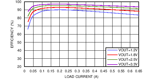
GUID-93F7AA6E-2E9B-499F-A45C-E5E3C20D377D-low.pngTypical Efficiency at VIN = 3.6 V
GUID-5D0E3396-CDB5-4B52-A1AB-7FA69C613D0C-low.pngRadiated EMI (CISPR22) VIN = 5 V, VOUT = 1.8 V, IOUT = 650 mA