SNVS633K January   2010  – April 2019 LMZ10505

PRODUCTION DATA.  

  1. Features
  2. Applications
  3. Description
    1.     Device Images
      1.      Typical Application Circuit
      2.      Efficiency VOUT = 3.3 V
  4. Revision History
  5. Pin Configuration and Functions
    1.     Pin Functions
  6. Specifications
    1. 6.1 Absolute Maximum Ratings
    2. 6.2 ESD Ratings
    3. 6.3 Recommended Operating Conditions
    4. 6.4 Thermal Information
    5. 6.5 Electrical Characteristics
    6. 6.6 Typical Characteristics
  7. Detailed Description
    1. 7.1 Overview
    2. 7.2 Functional Block Diagram
    3. 7.3 Feature Description
      1. 7.3.1 Enable
      2. 7.3.2 Enable and UVLO
      3. 7.3.3 Soft-Start
      4. 7.3.4 Soft-Start Capacitor
      5. 7.3.5 Tracking
      6. 7.3.6 Tracking - Equal Soft-Start Time
      7. 7.3.7 Tracking - Equal Slew Rates
      8. 7.3.8 Current Limit
      9. 7.3.9 Overtemperature Protection
    4. 7.4 Device Functional Modes
      1. 7.4.1 Prebias Start-Up Capability
  8. Application and Implementation
    1. 8.1 Application Information
    2. 8.2 Typical Application
      1. 8.2.1 Design Requirements
      2. 8.2.2 Detailed Design Procedure
        1. 8.2.2.1 Custom Design With WEBENCH® Tools
        2. 8.2.2.2 Input Capacitor Selection
        3. 8.2.2.3 Output Capacitor Selection
          1. 8.2.2.3.1 Output Voltage Setting
        4. 8.2.2.4 Loop Compensation
      3. 8.2.3 Application Curves
    3. 8.3 System Examples
      1. 8.3.1 Application Schematic for 3.3-V to 5-V Input and 2.5-V Output With Optimized Ripple and Transient Response
      2. 8.3.2 Application Schematic for 3.3-V to 5-V Input and 2.5-V Output
      3. 8.3.3 EMI Tested Schematic for 2.5-V Output Based on 3.3-V to 5-V Input
  9. Power Supply Recommendations
  10. 10Layout
    1. 10.1 Layout Guidelines
    2. 10.2 Layout Examples
    3. 10.3 Estimate Power Dissipation and Thermal Considerations
    4. 10.4 Power Module SMT Guidelines
  11. 11Device and Documentation Support
    1. 11.1 Device Support
      1. 11.1.1 Third-Party Products Disclaimer
      2. 11.1.2 Development Support
        1. 11.1.2.1 Custom Design With WEBENCH® Tools
    2. 11.2 Documentation Support
      1. 11.2.1 Related Documentation
    3. 11.3 Receiving Notification of Documentation Updates
    4. 11.4 Community Resources
    5. 11.5 Trademarks
    6. 11.6 Electrostatic Discharge Caution
    7. 11.7 Glossary
  12. 12Mechanical, Packaging, and Orderable Information

Package Options

Mechanical Data (Package|Pins)
Thermal pad, mechanical data (Package|Pins)
Orderable Information

Layout Examples

The PCB design is available in the LMZ10505 product folder at www.ti.com.
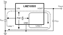
LMZ10505 30107453.gifFigure 29. Critical Current Loops to Minimize
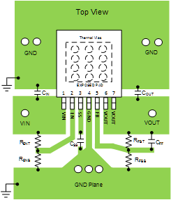
LMZ10505 TOPMOD_7pin_Layout_LMZ1050X.gifFigure 30. PCB Layout Guide
LMZ10505 30088276.pngFigure 31. Top Copper
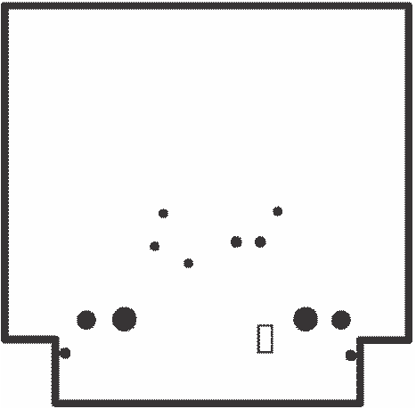
LMZ10505 30107477.pngFigure 32. Internal Layer 1 (Ground)
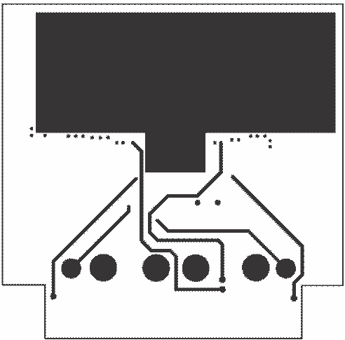
LMZ10505 30118378.pngFigure 33. Internal Layer 2 (Ground and Signal Traces)
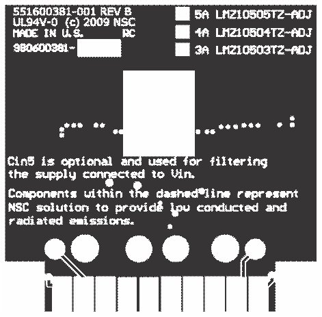
LMZ10505 30107479.pngFigure 34. Bottom Copper