SNVS633K January 2010 – April 2019 LMZ10505
PRODUCTION DATA.
- 1 Features
- 2 Applications
- 3 Description
- 4 Revision History
- 5 Pin Configuration and Functions
- 6 Specifications
- 7 Detailed Description
- 8 Application and Implementation
- 9 Power Supply Recommendations
- 10Layout
- 11Device and Documentation Support
- 12Mechanical, Packaging, and Orderable Information
Package Options
Mechanical Data (Package|Pins)
- NDW|7
Thermal pad, mechanical data (Package|Pins)
Orderable Information
8.2.2.4 Loop Compensation
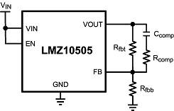
The LMZ10505 preserves flexibility by integrating the control components around the internal error amplifier while utilizing three small external compensation components from VOUT to FB. An integrated type II (two pole, one zero) voltage-mode compensation network is featured. To ensure stability, an external resistor and small value capacitor can be added across the upper feedback resistor as a pole-zero pair to complete a type III (three pole, two zero) compensation network. The compensation components recommended in Table 4 provide type III compensation at an optimal control loop performance. The typical phase margin is 45° with a bandwidth of 80 kHz. Calculated output capacitance values not listed in Table 4 should be verified before designing into production. The AN-2013 LMZ1050x/LMZ1050xEXT SIMPLE SWITCHER Power Module (SNVA417) is a detailed application note that provides verification support. In general, calculated output capacitance values below the suggested value will have reduced phase margin and higher control loop bandwidth. Output capacitance values above the suggested values will experience a lower bandwidth and increased phase margin. Higher bandwidth is associated with faster system response to sudden changes such as load transients. Phase margin changes the characteristics of the response. Lower phase margin is associated with underdamped ringing and higher phase margin is associated with overdamped response. Losing all phase margin will cause the system to be unstable; an optimized area of operation is 30° to 60° of phase margin, with a bandwidth of 100 kHz ±20 kHz.
 Figure 22. Loop Compensation Control Components
 Table 4. LMZ10505 Compensation Component Values
| VIN (V) | CO (µF) | ESR (mΩ) | Rfbt (kΩ)(1) | Ccomp (pF)(1) | Rcomp (kΩ)(1) | |
|---|---|---|---|---|---|---|
| MIN | MAX | |||||
| 5 | 22 | 2 | 20 | 200 | 27 | 1.5 |
| 47 | 2 | 20 | 124 | 68 | 1.4 | |
| 100 | 1 | 10 | 82.5 | 150 | 0.681 | |
| 150 | 1 | 5 | 63.4 | 220 | 1 | |
| 150 | 10 | 25 | 63.4 | 220 | 3.48 | |
| 150 | 26 | 50 | 226 | 62 | 12.1 | |
| 220 | 15 | 30 | 150 | 100 | 6.98 | |
| 220 | 31 | 60 | 316 | 560 | 14 | |
| 3.3 | 22 | 2 | 20 | 118 | 43 | 9.09 |
| 47 | 2 | 20 | 76.8 | 100 | 3.32 | |
| 100 | 1 | 10 | 49.9 | 180 | 2.49 | |
| 150 | 1 | 5 | 40.2 | 330 | 1 | |
| 150 | 10 | 25 | 43.2 | 330 | 4.99 | |
| 150 | 26 | 50 | 143 | 100 | 7.5 | |
| 220 | 15 | 30 | 100 | 180 | 4.99 | |
| 220 | 31 | 60 | 200 | 100 | 8.06 | |