SNVS709G March 2011 – December 2015 LMZ13610
PRODUCTION DATA.
- 1 Features
- 2 Applications
- 3 Description
- 4 Revision History
- 5 Pin Configuration and Functions
- 6 Specifications
- 7 Detailed Description
-
8 Application and Implementation
- 8.1 Application Information
- 8.2
Typical Application
- 8.2.1 Design Requirements
- 8.2.2
Detailed Design Procedure
- 8.2.2.1 Design Steps
- 8.2.2.2 Enable Divider, RENT, RENB and RENH Selection
- 8.2.2.3 Output Voltage Selection
- 8.2.2.4 Soft-Start Capacitor Selection
- 8.2.2.5 Tracking Supply Divider Option
- 8.2.2.6 COUT Selection
- 8.2.2.7 CIN Selection
- 8.2.2.8 Discontinuous Conduction and Continuous Conduction Modes Selection
- 8.2.3 Application Curves
- 9 Power Supply Recommendations
- 10Layout
- 11Device and Documentation Support
- 12Mechanical, Packaging, and Orderable Information
Package Options
Mechanical Data (Package|Pins)
- NDY|11
Thermal pad, mechanical data (Package|Pins)
Orderable Information
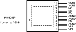
5 Pin Configuration and Functions
NDY Package
11-Pin
Top View

Pin Functions
| PIN | TYPE | DESCRIPTION | |
|---|---|---|---|
| NAME | NO. | ||
| AGND | 3 | Ground | Analog Ground — Reference point for all stated voltages. Must be externally connected to EP/PGND. |
| 5 | |||
| 6 | |||
| EN | 4 | Analog | Enable — Input to the precision enable comparator. Rising threshold is 1.274 V typical. Once the module is enabled, a 20-µA source current is internally activated to accommodate programmable hysteresis. |
| FB | 7 | Analog | Feedback — Internally connected to the regulation, overvoltage, and short circuit comparators. The regulation reference point is 0.8 V at this input pin. Connect the feedback resistor divider between the output and AGND to set the output voltage. |
| NC | 9 | — | No Connect. This pin must remain floating, do not ground. |
| PGND | — | Power | Exposed Pad / Power Ground Electrical path for the power circuits within the module. — NOT Internally connected to AGND / pin 5. Used to dissipate heat from the package during operation. Must be electrically connected to pin 5 external to the package. |
| SS | 8 | Analog | Soft-Start/Track input — To extend the 1.6-ms internal soft-start connect an external soft-start capacitor. For tracking connect to an external resistive divider connected to a higher priority supply rail. See Design Steps section. |
| VIN | 1 | Power | Supply input — Nominal operating range is 6 V to 36 V. A small amount of internal capacitance is contained within the package assembly. Additional external input capacitance is required between this pin and PGND. |
| 2 | |||
| VOUT | 10 | Power | Output Voltage — Output from the internal inductor. Connect the output capacitor between this pin and PGND. |
| 11 | |||