-
LMZ14202EXT 2-A SIMPLE SWITCHER® Power Module With 42-V Maximum Input Voltage for Demanding Environments and Rugged Applications
- 1 Features
- 2 Applications
- 3 Description
- 4 Revision History
- 5 Pin Configuration and Functions
- 6 Specifications
- 7 Detailed Description
- 8 Application and Implementation
- 9 Power Supply Recommendations
- 10Layout
- 11Device and Documentation Support
- 12Mechanical, Packaging, and Orderable Information
- IMPORTANT NOTICE
Package Options
Mechanical Data (Package|Pins)
- NDW|7
Thermal pad, mechanical data (Package|Pins)
Orderable Information
LMZ14202EXT 2-A SIMPLE SWITCHER® Power Module With 42-V Maximum Input Voltage for Demanding Environments and Rugged Applications
1 Features
- Junction Temperature Range –55°C to 125°C
- Integrated Shielded Inductor
- Simple PCB Layout
- Flexible Start-up Sequencing Using External Soft-Start and Precision Enable
- Protection Against Inrush Currents and Faults such as Input UVLO and Output Short Circuit
- Single Exposed Pad and Standard Pinout for Easy Mounting and Manufacturing
- Fast Transient Response for Powering FPGAs and ASICs
- Low Output Voltage Ripple
- Pin-to-Pin Compatible With Family Devices:
- LMZ14203EXT/2EXT/1EXT
(42-V Maximum 3 A, 2 A, 1 A) - LMZ14203/2/1 (42-V Maximum 3 A, 2 A, 1 A)
- LMZ12003/2/1 (20-V Maximum 3 A, 2 A, 1 A)
- LMZ14203EXT/2EXT/1EXT
- Fully Enabled for WEBENCH® Power Designer
- Electrical Specifications
- 12-W Maximum Total Output Power
- Up to 2-A Output Current
- Input Voltage Range 6 V to 42 V
- Output Voltage Range 0.8 V to 6 V
- Efficiency up to 90%
- Performance Benefits
- Low Radiated Emissions and High Radiated Immunity
- Passes Vibration Standard MIL-STD-883 Method 2007.2 Condition A JESD22–B103B Condition 1
- Passes Drop Standard MIL-STD-883 Method 2002.3 Condition B JESD22–B110 Condition B
2 Applications
- Point-of-load Conversions from 12-V and 24-V Input Rail
- Time Critical Projects
- Space Constrained and High Thermal Requirement Applications
- Negative Output Voltage Applications
(See AN-2027 SNVA425)
3 Description
The LMZ14202EXT SIMPLE SWITCHER® power module is an easy-to-use step-down DC-DC solution capable of driving up to 2-A load with exceptional power conversion efficiency, line and load regulation, and output accuracy. The LMZ14202EXT is available in an innovative package that enhances thermal performance and allows for hand or machine soldering.
The LMZ14202EXT can accept an input voltage rail between 6 V and 42 V and can deliver an adjustable and highly accurate output voltage as low as 0.8 V. The LMZ14202EXT only requires three external resistors and four external capacitors to complete the power solution. The LMZ14202EXT is a reliable and robust design with the following protection features: thermal shutdown, input undervoltage lockout, output overvoltage protection, short-circuit protection, output current limit, and the device allows start-up into a prebiased output. A single resistor adjusts the switching frequency up to 1 MHz.
Device Information(1)(2)
| PART NUMBER | PACKAGE | BODY SIZE (NOM) |
|---|---|---|
| LMZ14202EXT | TO-PMOD (7) | 10.16 mm × 9.85 mm |
- For all available packages, see the orderable addendum at the end of the data sheet.
- Peak reflow temperature equals 245°C. See SNAA214 for more details.
Simplified Application Schematic

Efficiency 12-V Input at 25°C

4 Revision History
Changes from G Revision (August 2015) to H Revision
- Added this ne bullet the Power Module SMT Guidelines sectionGo
Changes from F Revision (October 2013) to G Revision
- Added Pin Configuration and Functions section, ESD Ratings table, Feature Description section, Device Functional Modes, Application and Implementation section, Power Supply Recommendations section, Layout section, Device and Documentation Support section, and Mechanical, Packaging, and Orderable Information sectionGo
- Removed Easy-to-Use PFM 7-Pin Package imageGo
Changes from E Revision (April 2013) to F Revision
5 Pin Configuration and Functions

Pin Functions
| PIN | TYPE | DESCRIPTION | |
|---|---|---|---|
| NAME | NO. | ||
| EN | 3 | Analog | Enable — Input to the precision enable comparator. Rising threshold is 1.18 V nominal; 90 mV hysteresis nominal. Maximum recommended input level is 6.5 V. |
| EP | — | Ground | Exposed Pad — Internally connected to pin 4. Used to dissipate heat from the package during operation. Must be electrically connected to pin 4 external to the package. |
| FB | 6 | Analog | Feedback — Internally connected to the regulation, overvoltage, and short-circuit comparators. The regulation reference point is 0.8 V at this input pin. Connected the feedback resistor divider between the output and ground to set the output voltage. |
| GND | 4 | Ground | Ground — Reference point for all stated voltages. Must be externally connected to EP. |
| RON | 2 | Analog | ON-Time Resistor — An external resistor from VIN to this pin sets the ON-time of the application. Typical values range from 25 kΩ to 124 kΩ. |
| SS | 5 | Analog | Soft-Start — An internal 8-µA current source charges an external capacitor to produce the soft-start function. This node is discharged at 200 µA during disable, overcurrent, thermal shutdown and internal UVLO conditions. |
| VIN | 1 | Power | Supply input — Nominal operating range is 6 V to 42 V. A small amount of internal capacitance is contained within the package assembly. Additional external input capacitance is required between this pin and exposed pad. |
| VOUT | 7 | Power | Output Voltage — Output from the internal inductor. Connect the output capacitor between this pin and exposed pad. |
6 Specifications
6.1 Absolute Maximum Ratings
over operating free-air temperature range (unless otherwise noted)(1)(2)| MIN | MAX | UNIT | |
|---|---|---|---|
| VIN, RON to GND | –0.3 | 43.5 | V |
| EN, FB, SS to GND | –0.3 | 7 | V |
| Junction temperature | 150 | °C | |
| Peak reflow case temperature (30 sec) | 245 | °C | |
| Storage temperature | –65 | 150 | °C |
6.2 ESD Ratings
| VALUE | UNIT | |||
|---|---|---|---|---|
| V(ESD) | Electrostatic discharge | Human body model (HBM), per ANSI/ESDA/JEDEC JS-001(1)(2) | ±2000 | V |
6.3 Recommended Operating Conditions
over operating free-air temperature range (unless otherwise noted)| MIN | MAX | UNIT | |
|---|---|---|---|
| VIN | 6 | 42 | V |
| EN | 0 | 6.5 | V |
| Operation Junction Temperature | −55 | 125 | °C |
6.4 Thermal Information
| THERMAL METRIC(1) | LMZ14202EXT | UNIT | ||
|---|---|---|---|---|
| NDW (TO-PMOD) | ||||
| 7 PINS | ||||
| RθJA | Junction-to-ambient thermal resistance(2) | 4-layer JEDEC Printed-Circuit-Board, 100 vias, No air flow | 19.3 | °C/W |
| 2-layer JEDEC Printed-Circuit-Board, No air flow | 21.5 | |||
| RθJC(top) | Junction-to-case (top) thermal resistance | No air flow | 1.9 | °C/W |
6.5 Electrical Characteristics
Limits in standard type are for TJ = 25°C, unless otherwise specified. Minimum and Maximum limits are ensured through test, design or statistical correlation. Typical values represent the most likely parametric norm at TJ = 25°C, and are provided for reference purposes only. Unless otherwise stated the following conditions apply: VIN = 24 V, VOUT = 3.3 V.| PARAMETER | TEST CONDITIONS | MIN(1) | TYP(2) | MAX(1) | UNIT | ||
|---|---|---|---|---|---|---|---|
| SYSTEM PARAMETERS | |||||||
| ENABLE CONTROL(3) | |||||||
| VEN | EN threshold trip point | VEN rising | 1.18 | V | |||
| over the junction temperature (TJ) range of –55°C to +125°C | 1.1 | 1.26 | |||||
| VEN-HYS | EN threshold hysteresis | VEN falling | 90 | mV | |||
| SOFT-START | |||||||
| ISS | SS source current | VSS = 0 V | 8 | µA | |||
| over the junction temperature (TJ) range of –55°C to +125°C | 4.9 | 11 | |||||
| ISS-DIS | SS discharge current | –200 | µA | ||||
| CURRENT LIMIT | |||||||
| ICL | Current limit threshold | DC average | 2.6 | A | |||
| over the junction temperature (TJ) range of –55°C to +125°C | 2.3 | 3.65 | |||||
| REGULATION AND OVERVOLTAGE COMPARATOR | |||||||
| VFB | In-regulation feedback voltage | VSS >+ 0.8 V TJ = –55°C to 125°C IO = 2 A |
0.795 | V | |||
| over the junction temperature (TJ) range of –55°C to +125°C | 0.775 | 0.815 | |||||
| VSS >+ 0.8 V TJ = 25°C IO = 10 mA |
0.786 | 0.802 | 0.818 | V | |||
| VFB-OV | Feedback overvoltage protection threshold | 0.92 | V | ||||
| IFB | Feedback input bias current | 5 | nA | ||||
| IQ | Non-switching input current | VFB = 0.86 V | 1 | mA | |||
| ISD | Shutdown quiescent current | VEN = 0 V | 25 | μA | |||
| THERMAL CHARACTERISTICS | |||||||
| TSD | Thermal shutdown | Rising | 165 | °C | |||
| TSD-HYST | Thermal shutdown hysteresis | Falling | 15 | °C | |||
| PERFORMANCE PARAMETERS | |||||||
| ΔVO | Output voltage ripple | 8 | mVPP | ||||
| ΔVO/ΔVIN | Line regulation | VIN = 12 V to 42 V, IO = 2 A | 0.01% | ||||
| ΔVO/IOUT | Load regulation | VIN = 24 V | 1.5 | mV/A | |||
| η | Efficiency | VIN = 24 V, VO = 3.3 V, IO = 1 A | 86% | ||||
| VIN = 24 V, VO = 3.3 V, IO = 2 A | 85% | ||||||
6.6 Switching Characteristics
over operating free-air temperature range (unless otherwise noted)| PARAMETER | TEST CONDITIONS | MIN | TYP | MAX | UNIT | |
|---|---|---|---|---|---|---|
| ON/OFF TIMER | ||||||
| tON-MIN | ON timer minimum pulse width | 150 | ns | |||
| tOFF | OFF timer pulse width | 260 | ns | |||
6.7 Typical Characteristics
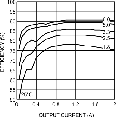
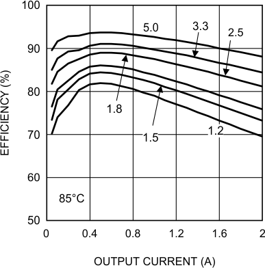
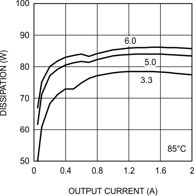
Unless otherwise specified, the following conditions apply: VIN = 24 V; CIN = 10-µF X7R Ceramic; CO = 100-µF X7R Ceramic; TA = 25°C for efficiency curves and waveforms.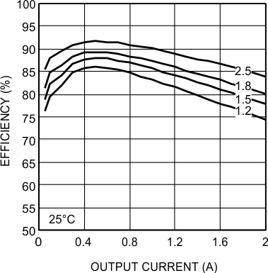







24-VIN 3.3-VO 0.6-A to 2-A Step
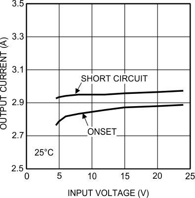
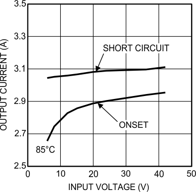
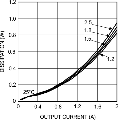

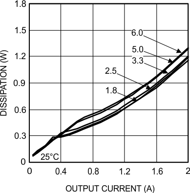

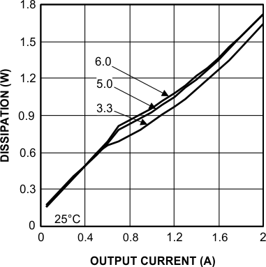
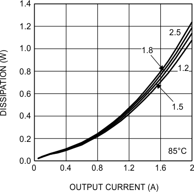
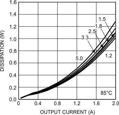

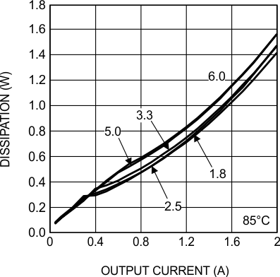


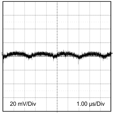
24-VIN 3.3-VO 2A, BW = 200 MHz


7 Detailed Description
7.1 Overview
7.1.1 COT Control Circuit Overview
Constant ON-Time control is based on a comparator and an ON-time, one-shot with the output voltage feedback compared with an internal 0.8-V reference. If the feedback voltage is below the reference, the main MOSFET is turned on for a fixed ON-time determined by a programming resistor RON. RON is connected to VIN such that ON-time is reduced with increasing input supply voltage. Following this ON-time, the main MOSFET remains off for a minimum of 260 ns. If the voltage on the feedback pin falls below the reference level again the ON-time cycle is repeated. Regulation is achieved in this manner.
7.2 Functional Block Diagram

7.3 Feature Description
7.3.1 Output Overvoltage Comparator
The voltage at FB is compared to a 0.92-V internal reference. If FB rises above 0.92 V, the ON-time is immediately terminated. This condition is known as overvoltage protection (OVP). It can occur if the input voltage is increased very suddenly or if the output load is decreased very suddenly. When OVP is activated, the top MOSFET ON-times will be inhibited until the condition clears. Additionally, the synchronous MOSFET will remain on until inductor current falls to zero.
7.3.2 Current Limit
Current limit detection is carried out during the OFF-time by monitoring the current in the synchronous MOSFET. Referring to the Functional Block Diagram, when the top MOSFET is turned off, the inductor current flows through the load, the PGND pin and the internal synchronous MOSFET. If this current exceeds 2.6 A (typical) the current limit comparator disables the start of the next ON-time period. The next switching cycle will occur only if the FB input is less than 0.8 V and the inductor current has decreased below 2.6 A. Inductor current is monitored during the period of time the synchronous MOSFET is conducting. So long as inductor current exceeds 2.6 A, further ON-time intervals for the top MOSFET will not occur. Switching frequency is lower during current limit due to the longer OFF-time. It must also be noted that current limit is dependent on both duty cycle and temperature as illustrated in the graphs in the Typical Characteristics.
7.3.3 Thermal Protection
The junction temperature of the LMZ14202EXT must not be allowed to exceed its maximum ratings. Thermal protection is implemented by an internal Thermal Shutdown circuit which activates at 165°C (typical) causing the device to enter a low-power standby state. In this state the main MOSFET remains off causing VO to fall, and additionally the CSS capacitor is discharged to ground. Thermal protection helps prevent catastrophic failures for accidental device overheating. When the junction temperature falls back below 145°C (typical hysteresis = 20°C) the SS pin is released, VO rises smoothly, and normal operation resumes.
Applications requiring maximum output current especially those at high-input voltage may require application derating at elevated temperatures.
7.3.4 Zero Coil Current Detection
The current of the lower (synchronous) MOSFET is monitored by a zero coil current detection circuit which inhibits the synchronous MOSFET when its current reaches zero until the next ON-time. This circuit enables the DCM operating mode, which improves efficiency at light loads.
7.3.5 Prebiased Start-Up
The LMZ14202EXT will properly start up into a prebiased output. This start-up situation is common in multiple rail logic applications where current paths may exist between different power rails during the start-up sequence. The following scope capture shows proper behavior during this event.
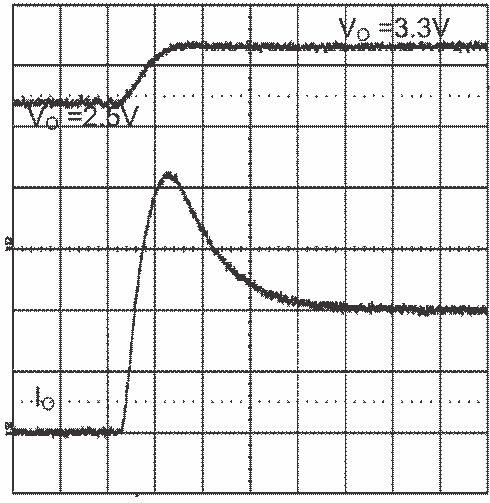 Figure 33. Prebiased Start-Up
7.4 Device Functional Modes
7.4.1 Discontinuous Conduction and Continuous Conduction Modes Selection
At light load, the regulator will operate in discontinuous conduction mode (DCM). With load currents above the critical conduction point, it will operate in continuous conduction mode (CCM). When operating in DCM the switching cycle begins at zero amps inductor current; increases up to a peak value, and then recedes back to zero before the end of the OFF-time. Note that during the period of time that inductor current is zero, all load current is supplied by the output capacitor. The next ON-time period starts when the voltage on the at the FB pin falls below the internal reference. The switching frequency is lower in DCM and varies more with load current as compared to CCM. Conversion efficiency in DCM is maintained because conduction and switching losses are reduced with the smaller load and lower switching frequency.
8 Application and Implementation
NOTE
Information in the following applications sections is not part of the TI component specification, and TI does not warrant its accuracy or completeness. TI’s customers are responsible for determining suitability of components for their purposes. Customers should validate and test their design implementation to confirm system functionality.
8.1 Application Information
The LMZ14202EXT is a step-down DC-to-DC power module. It is typically used to convert a higher DC voltage to a lower DC voltage with a maximum output current of 2 A. The following design procedure can be used to select components for the LMZ14202EXT. Alternately, the WEBENCH software may be used to generate complete designs.
When generating a design, the WEBENCH software utilizes iterative design procedure and accesses comprehensive databases of components.
8.2 Typical Application
 Figure 34. Evaluation Board Schematic Diagram
Table 1. Bill of Materials
| REF DES | DESCRIPTION | CASE SIZE | MANUFACTURER | MANUFACTURER P/N |
|---|---|---|---|---|
| U1 | SIMPLE SWITCHER | PFM-7 | Texas Instruments | LMZ14202EXTTZ-ADJ |
| Cin1 | 1 µF, 50 V, X7R | 1206 | Taiyo Yuden | UMK316B7105KL-T |
| Cin2 | 10 µF, 50 V, X7R | 1210 | Taiyo Yuden | UMK325BJ106MM-T |
| CO1 | 1 µF, 50 V, X7R | 1206 | Taiyo Yuden | UMK316B7105KL-T |
| CO2 | 100 µF, 6.3 V, X7R | 1210 | Taiyo Yuden | JMK325BJ107MM-T |
| RFBT | 3.32 kΩ | 0603 | Vishay Dale | CRCW06033K32FKEA |
| RFBB | 1.07 kΩ | 0603 | Vishay Dale | CRCW06031K07FKEA |
| RON | 61.9 kΩ | 0603 | Vishay Dale | CRCW060361k9FKEA |
| RENT | 68.1 kΩ | 0603 | Vishay Dale | CRCW060368k1FKEA |
| RENB | 11.8 kΩ | 0603 | Vishay Dale | CRCW060311k8FKEA |
| CFF | 22 nF, ±10%, X7R, 16 V | 0603 | TDK | C1608X7R1H223K |
| CSS | 22 nF, ±10%, X7R, 16 V | 0603 | TDK | C1608X7R1H223K |
8.2.1 Design Requirements
For this example, the following application parameters exist:
- VIN Range = up to 42 V
- VOUT = 0.8 V to 6 V
- IOUT = 2 A
8.2.2 Detailed Design Procedure
8.2.2.1 Design Steps for the LMZ14202EXT Application
The LMZ14202EXT is fully supported by WEBENCH and offers the following: component selection, electrical and thermal simulations, as well as the build-it board for a reduction in design time. The following list of steps can be used to manually design the LMZ14202EXT application.
- Select minimum operating VIN with enable divider resistors
- Program VO with divider resistor selection
- Program turnon time with soft-start capacitor selection
- Select CO
- Select CIN
- Set operating frequency with RON
- Determine module dissipation
- Layout PCB for required thermal performance
8.2.2.1.1 Enable Divider, RENT and RENB Selection
The enable input provides a precise 1.18-V band-gap rising threshold to allow direct logic drive or connection to a voltage divider from a higher enable voltage such as VIN. The enable input also incorporates 90 mV (typical) of hysteresis resulting in a falling threshold of 1.09 V. The maximum recommended voltage into the EN pin is 6.5 V. For applications where the midpoint of the enable divider exceeds 6.5 V, a small Zener diode can be added to limit this voltage.
The function of this resistive divider is to allow the designer to choose an input voltage below which the circuit will be disabled. This implements the feature of programmable under voltage lockout. This is often used in battery powered systems to prevent deep discharge of the system battery. It is also useful in system designs for sequencing of output rails or to prevent early turnon of the supply as the main input voltage rail rises at power-up. Applying the enable divider to the main input rail is often done in the case of higher input voltage systems such as 24-V AC/DC systems where a lower boundary of operation must be established. In the case of sequencing supplies, the divider is connected to a rail that becomes active earlier in the power-up cycle than the LMZ14202EXT output rail. The two resistors must be chosen based on the following ratio:
The LMZ14202EXT demonstration and evaluation boards use 11.8 kΩ for RENB and 68.1 kΩ for RENT resulting in a rising UVLO of 8 V. This divider presents 6.25 V to the EN input when the divider input is raised to 42 V.
8.2.2.1.2 Output Voltage Selection
Output voltage is determined by a divider of two resistors connected between VO and ground. The midpoint of the divider is connected to the FB input. The voltage at FB is compared to a 0.8-V internal reference. In normal operation an ON-time cycle is initiated when the voltage on the FB pin falls below 0.8 V. The main MOSFET ON-time cycle causes the output voltage to rise and the voltage at the FB to exceed 0.8 V. As long as the voltage at FB is above 0.8 V, ON-time cycles will not occur.
The regulated output voltage determined by the external divider resistors RFBT and RFBB is:
Rearranging terms; the ratio of the feedback resistors for a desired output voltage is:
These resistors must be chosen from values in the range of 1 kΩ to 10 kΩ.
For VO = 0.8 V the FB pin can be connected to the output directly so long as an output preload resistor remains that draws more than 20 µA. Converter operation requires this minimum load to create a small inductor ripple current and maintain proper regulation when no load is present.
A feed-forward capacitor is placed in parallel with RFBT to improve load step transient response. Its value is usually determined experimentally by load stepping between DCM and CCM conduction modes and adjusting for best transient response and minimum output ripple.
Table 1 is a table of values for RFBT , RFBB , CFF and RON.
8.2.2.1.3 Soft-Start Capacitor Selection
Programmable soft-start permits the regulator to slowly ramp to its steady state operating point after being enabled, thereby reducing current inrush from the input supply and slowing the output voltage rise-time to prevent overshoot.
Upon turnon, after all UVLO conditions have been passed, an internal 8-µA current source begins charging the external soft-start capacitor. The soft-start time duration to reach steady-state operation is given by the formula:
This equation can be rearranged as follows:
Use of a 0.022-μF capacitor results in 2.2-ms soft-start duration which is recommended as a minimum value.
As the soft-start input exceeds 0.8 V, the output of the power stage will be in regulation. The soft-start capacitor continues charging until it reaches approximately 3.8 V on the SS pin. Voltage levels between 0.8 V and 3.8 V have no effect on other circuit operation. The following conditions will reset the soft-start capacitor by discharging the SS input to ground with an internal 200-μA current sink:
- The enable input being pulled low
- Thermal shutdown condition
- Overcurrent fault
- Internal VCC UVLO (Approx 4-V input to VIN)
8.2.2.1.4 CO Selection
None of the required CO output capacitance is contained within the module. At a minimum, the output capacitor must meet the worst case minimum ripple current rating of 0.5 × ILRP-P, as calculated in Equation 18. Beyond that, additional capacitance will reduce output ripple so long as the ESR is low enough to permit it. A minimum value of 10 μF is generally required. Experimentation will be required if attempting to operate with a minimum value. Ceramic capacitors or other low ESR types are recommended. See AN-2024 SNVA422 for more detail.
The following equation provides a good first pass approximation of CO for load transient requirements:
Solving for Equation 6 yields the following:
The LMZ14202EXT demonstration and evaluation boards are populated with a 100-µF, 6.3-V X5R output capacitor. Locations for extra output capacitors are provided (see AN-2024 SNVA422 for locations).
8.2.2.1.5 CIN Selection
The LMZ14202EXT module contains an internal 0.47 µF input ceramic capacitor. Additional input capacitance is required external to the module to handle the input ripple current of the application. This input capacitance must be located in very close proximity to the module. Input capacitor selection is generally directed to satisfy the input ripple current requirements rather than by capacitance value. Worst case input ripple current rating is dictated by the equation:
where
- D ≊ VO / VIN
As a point of reference, the worst case ripple current will occur when the module is presented with full load current and when VIN = 2 × VO.
Recommended minimum input capacitance is 10-µF X7R ceramic with a voltage rating at least 25% higher than the maximum applied input voltage for the application. Pay attention to the voltage and temperature deratings of the capacitor selected. Ripple current rating of ceramic capacitors may be missing from the capacitor data sheet and you may have to contact the capacitor manufacturer for this rating.
If the system design requires a certain minimum value of input ripple voltage ΔVIN be maintained then the following equation may be used.
If ΔVIN is 1% of VIN for a 24-V input to 3.3-V output application this equals 240 mV and fSW = 400 kHz.
Additional bulk capacitance with higher ESR may be required to damp any resonant effects of the input capacitance and parasitic inductance of the incoming supply lines.
8.2.2.1.6 RON Resistor Selection
Many designs will begin with a desired switching frequency in mind. For that purpose the following equation can be used.
This can be rearranged as
The selection of RON and fSW(CCM) must be confined by limitations in the ON-time and OFF-time for the COT control section.
The ON-time of the LMZ14202EXT timer is determined by the resistor RON and the input voltage VIN. It is calculated as follows:
The inverse relationship of tON and VIN gives a nearly constant switching frequency as VIN is varied. RON must be selected such that the ON-time at maximum VIN is greater than 150 ns. The ON-timer has a limiter to ensure a minimum of 150 ns for tON. This limits the maximum operating frequency, which is governed by the following equation:
This equation can be used to select RON if a certain operating frequency is desired so long as the minimum ON-time of 150 ns is observed. The limit for RON can be calculated as follows:
If RON calculated in Equation 12 is less than the minimum value determined in Equation 15 a lower frequency must be selected. Alternatively, VIN(MAX) can also be limited in order to keep the frequency unchanged.
Additionally, consider that the minimum OFF-time of 260 ns limits the maximum duty ratio. Larger RON (lower FSW) must be selected in any application requiring large duty ratio.
8.2.2.1.6.1 Discontinuous Conduction and Continuous Conduction Modes Selection
Operating frequency in DCM can be calculated as follows:
In CCM, current flows through the inductor through the entire switching cycle and never falls to zero during the OFF-time. The switching frequency remains relatively constant with load current and line voltage variations. The CCM operating frequency can be calculated using Equation 11.
Figure 35 shows a comparison pair of waveforms of the showing both CCM (upper) and DCM operating modes.
 Figure 35. CCM and DCM Operating Modes
 VIN = 24 V, VO = 3.3 V, IO = 2 A / 0.32 A 2 μs/div
The approximate formula for determining the DCM/CCM boundary is as follows:
Figure 36 shows a typical waveform showing the boundary condition.
 Figure 36. Transition Mode Operation
VIN = 24 V, VO = 3.3 V, IO = 0.35 A 2 μs/div
The inductor internal to the module is 10 μH. This value was chosen as a good balance between low and high input voltage applications. The main parameter affected by the inductor is the amplitude of the inductor ripple current (ILR). ILR can be calculated with:
where
- VIN is the maximum input voltage
- fSW is determined from Equation 11
If the output current IO is determined by assuming that IO = IL, the higher and lower peak of ILR can be determined. Be aware that the lower peak of ILR must be positive if CCM operation is required.
8.2.3 Application Curves
 Figure 37. Efficiency VIN = 24 V VOUT = 5 V
 Figure 39. Radiated Emissions (EN 55022 Class B)
from Evaluation Board
 Figure 38. Thermal Derating Curve
VIN = 24 V, VOUT = 5 V,