SNVS874E August 2012 – September 2021 LMZ20501
PRODUCTION DATA
- 1 Features
- 2 Applications
- 3 Description
- 4 Revision History
- 5 Pin Configuration and Functions
- 6 Specifications
- 7 Detailed Description
- 8 Application and Implementation
- 9 Power Supply Recommendations
- 10Layout
- 11Device and Documentation Support
- 12Mechanical, Packaging, and Orderable Information
Package Options
Refer to the PDF data sheet for device specific package drawings
Mechanical Data (Package|Pins)
- SIL|8
Thermal pad, mechanical data (Package|Pins)
Orderable Information
10.2.1 Soldering Information
Proper operation of the LMZ20501 requires that it be correctly soldered to the PCB. This is especially true regarding the EP. This pad acts as a quiet ground reference for the device and a heatsink connection. Use the following recommendations when utilizing machine placement of the device:
- Dimension of area for pickup: 2 mm × 2.5 mm
- Use a nozzle size of less than 1.3 mm in diameter, so that the head does not touch the outer area of the package.
- Use a soft tip pick-and-place head.
- Add 0.05 mm to the component thickness so that the device will be released 0.05 mm into the solder paste without putting pressure or splashing the solder paste.
- Slow the pick arm when picking the part from the tape and reel carrier and when depositing the device on the board.
- If the machine releases the component by force, use the minimum force and no more than 3 N.
- For PCBs with surface mount components on both sides, it is suggested to put the LMZ20501 on the top side. In case the application requires bottom side placement, a re-flow fixture can be required to protect the module during the second reflow.
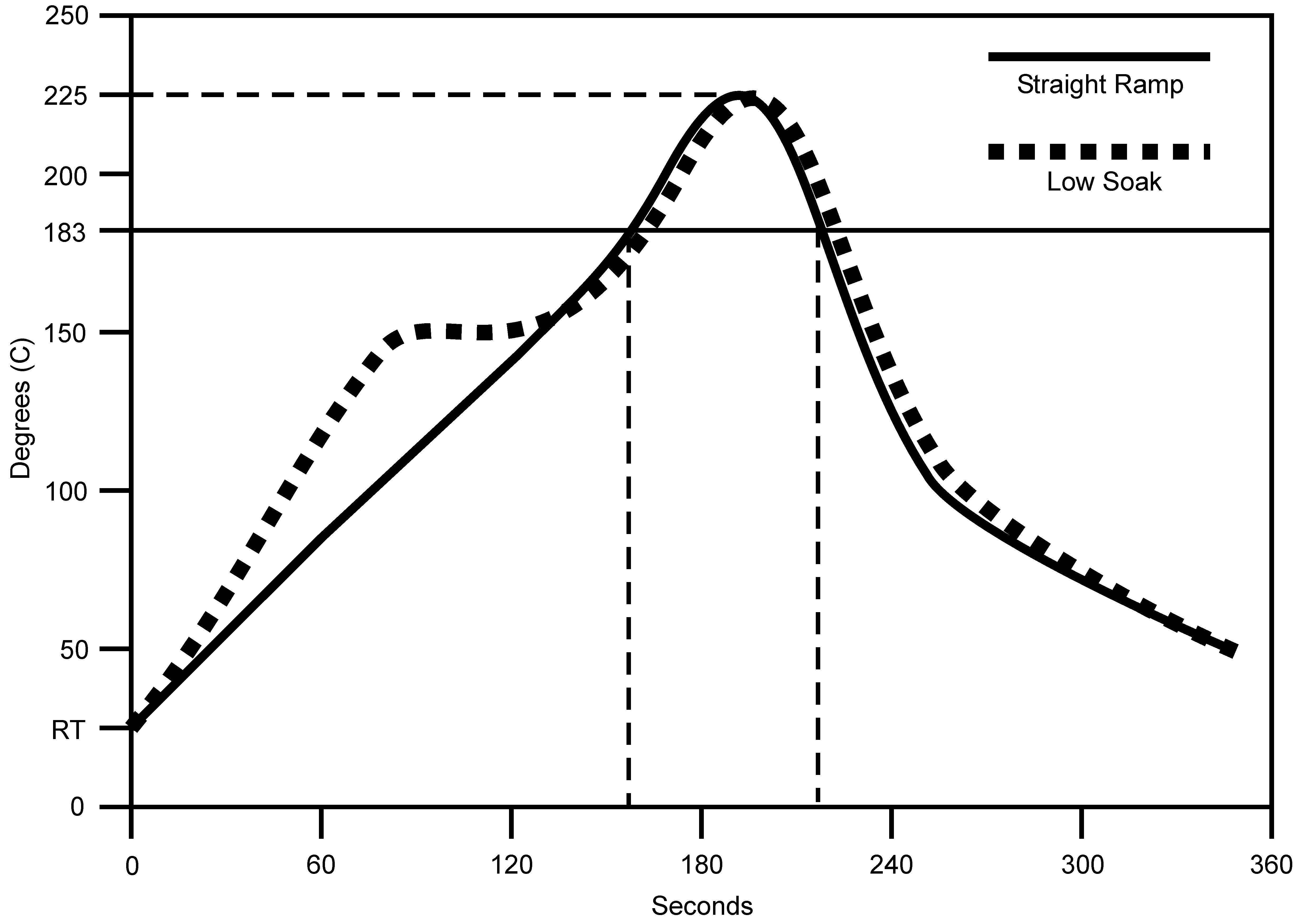
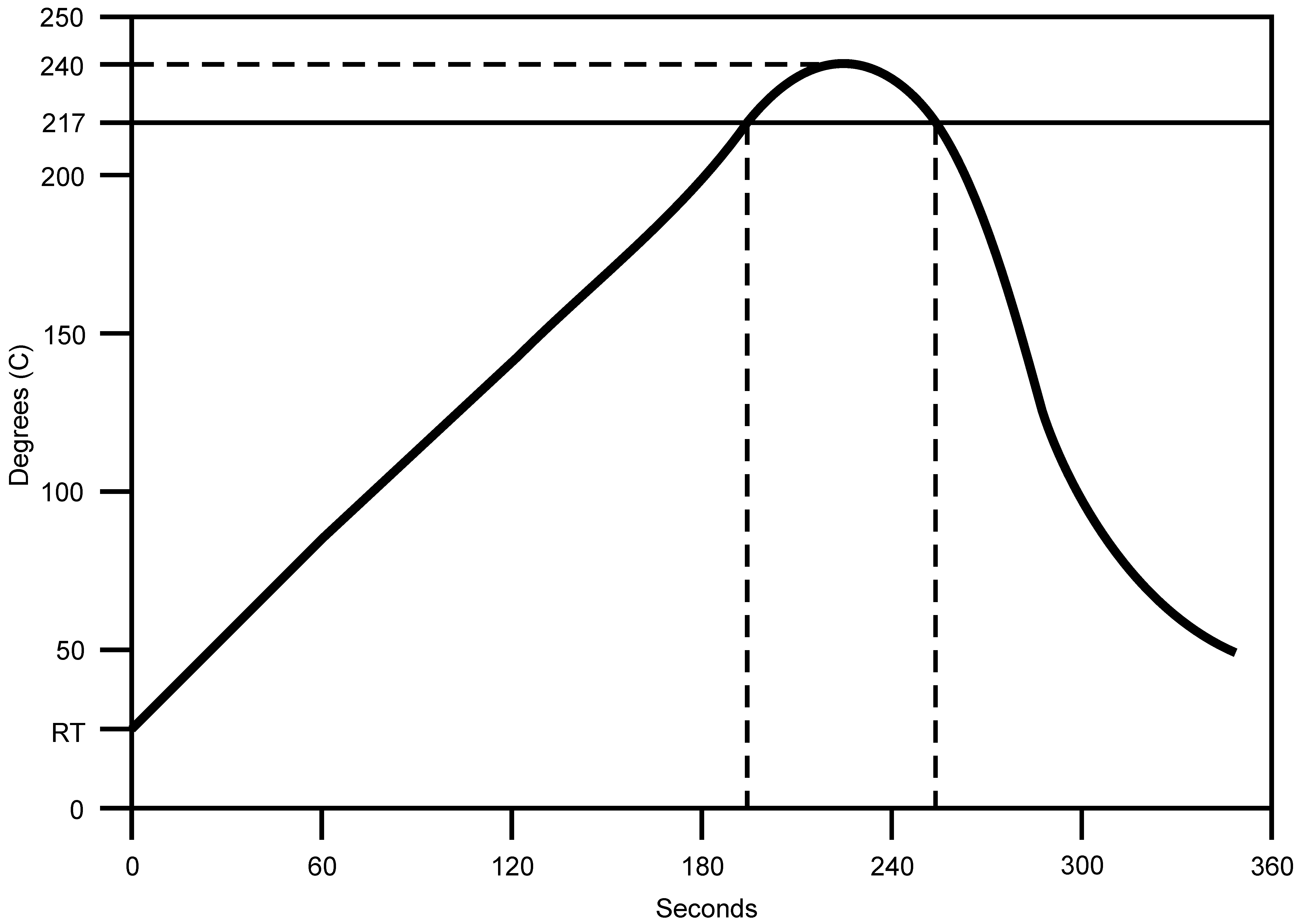
In addition, please follow the important guidelines found in the AN-1187 Leadless Leadframe Package (LLP) Application Report. The curves in Figure 10-3 and Figure 10-4 show typical soldering temperature profiles.
 Figure 10-3 Typical Re-flow Profile Eutectic (63sn/37pb) Solder Paste
 Figure 10-4 Typical Re-flow Profile Lead-Free (Sca305 Or Sac405) Solder Paste