SNVS874E August   2012  – September 2021 LMZ20501

PRODUCTION DATA  

  1. Features
  2. Applications
  3. Description
  4. Revision History
  5. Pin Configuration and Functions
  6. Specifications
    1. 6.1 Absolute Maximum Ratings
    2. 6.2 ESD Ratings
    3. 6.3 Recommended Operating Conditions
    4. 6.4 Thermal Information
    5. 6.5 Electrical Characteristics
    6. 6.6 System Characteristics
    7. 6.7 Typical Characteristics
  7. Detailed Description
    1. 7.1 Overview
    2. 7.2 Functional Block Diagram
    3. 7.3 Feature Description
      1. 7.3.1 Nano Scale Package
      2. 7.3.2 Internal Synchronous Rectifier
      3. 7.3.3 Current Limit Protection
      4. 7.3.4 Start-Up
      5. 7.3.5 Dropout Behavior
      6. 7.3.6 Power Good Flag Function
      7. 7.3.7 Thermal Shutdown
    4. 7.4 Device Functional Modes
      1. 7.4.1 PWM Operation
      2. 7.4.2 PFM Operation
  8. Application and Implementation
    1. 8.1 Application Information
    2. 8.2 Typical Application
      1. 8.2.1 Detailed Design Procedure
        1. 8.2.1.1 Custom Design With WEBENCH® Tools
        2. 8.2.1.2 Setting The Output Voltage
        3. 8.2.1.3 Output and Feedforward Capacitors
        4. 8.2.1.4 Input Capacitors
        5. 8.2.1.5 Maximum Ambient Temperature
        6. 8.2.1.6 Options
      2. 8.2.2 Application Curves
    3. 8.3 Do's and Don'ts
  9. Power Supply Recommendations
  10. 10Layout
    1. 10.1 Layout Guidelines
    2. 10.2 Layout Example
      1. 10.2.1 Soldering Information
  11. 11Device and Documentation Support
    1. 11.1 Device Support
      1. 11.1.1 Third-Party Products Disclaimer
      2. 11.1.2 Development Support
        1. 11.1.2.1 Custom Design With WEBENCH® Tools
    2. 11.2 Documentation Support
      1. 11.2.1 Related Documentation
    3. 11.3 Receiving Notification of Documentation Updates
    4. 11.4 Support Resources
    5. 11.5 Trademarks
    6. 11.6 Electrostatic Discharge Caution
    7. 11.7 Glossary
  12. 12Mechanical, Packaging, and Orderable Information
    1. 12.1 Tape and Reel Information

Package Options

Refer to the PDF data sheet for device specific package drawings

Mechanical Data (Package|Pins)
  • SIL|8
Thermal pad, mechanical data (Package|Pins)
Orderable Information

Description

The LMZ20501 nano module regulator is an easy-to-use synchronous step-down DC/DC converter capable of driving up to 1 A of load from an input of up to 5.5 V, with exceptional efficiency and output accuracy in a very small solution size. The innovative package contains the regulator and inductor in a small 3.5 mm × 3.5 mm × 1.75 mm volume, thus saving board space and eliminating the time and expense of inductor selection. The LMZ20501 requires only five external components and has a pin-out designed for simple, optimum PCB layout. The device provides for an easy to use complete design with a minimum number of external components and the TI WEBENCH® design tool. TI's WEBENCH tool includes features such as external component calculation, electrical simulation, and WebTherm®. For soldering information, see SNOA401.

Device Information
PART NUMBER PACKAGE(1) BODY SIZE (NOM)
LMZ20501 USIP (8) 3.50 mm × 3.50 mm
For all available packages, see the orderable addendum at the end of the data sheet.
GUID-F6E54DAF-2878-44CC-8A19-92DB93EA0590-low.gifSimplified Schematic
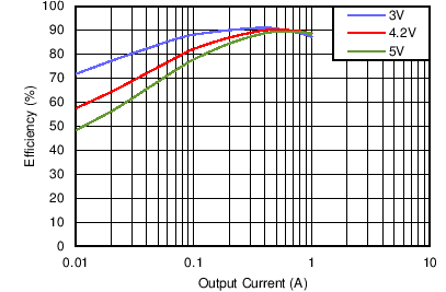
GUID-4C0758B9-A009-42C7-90B4-F8A19990C17B-low.pngTypical Efficiency for VOUT = 1.8 V Auto Mode