SNVS853E August   2012  – August 2018 LMZ21701

PRODUCTION DATA.  

  1. Features
  2. Applications
  3. Description
    1.     Device Images
      1.      Simplified Schematic
      2.      Efficiency for VIN = 12 V
  4. Revision History
  5. Pin Configuration and Functions
    1.     Pin Functions
  6. Specifications
    1. 6.1 Absolute Maximum Ratings
    2. 6.2 ESD Ratings
    3. 6.3 Recommended Operating Conditions
    4. 6.4 Thermal Information
    5. 6.5 Electrical Characteristics
    6. 6.6 Typical Characteristics
  7. Detailed Description
    1. 7.1 Overview
    2. 7.2 Functional Block Diagram
    3. 7.3 Package Construction
    4. 7.4 Feature Description
      1. 7.4.1 Input Undervoltage Lockout
      2. 7.4.2 Enable Input (EN)
      3. 7.4.3 Soft Start and Tracking Function (SS)
      4. 7.4.4 Power Good Function (PG)
      5. 7.4.5 Output Voltage Setting
      6. 7.4.6 Output Current Limit and Output Short Circuit Protection
      7. 7.4.7 Thermal Protection
    5. 7.5 Device Functional Modes
      1. 7.5.1 PWM Mode Operation
      2. 7.5.2 PSM Operation
  8. Application and Implementation
    1. 8.1 Application Information
    2. 8.2 Typical Application
      1. 8.2.1 Design Requirements
      2. 8.2.2 Detailed Design Procedure
        1. 8.2.2.1 Custom Design With WEBENCH® Tools
        2. 8.2.2.2 Input Capacitor (CIN)
        3. 8.2.2.3 Output Capacitor (COUT)
        4. 8.2.2.4 Soft-start Capacitor (CSS)
        5. 8.2.2.5 Power Good Resistor (RPG)
        6. 8.2.2.6 Feedback Resistors (RFBB and RFBT)
      3. 8.2.3 Application Curves
        1. 8.2.3.1 VOUT = 1.2 V
        2. 8.2.3.2 VOUT = 1.8 V
        3. 8.2.3.3 VOUT = 2.5 V
        4. 8.2.3.4 VOUT = 3.3 V
        5. 8.2.3.5 VOUT = 5.0 V
    3. 8.3 Do's and Don'ts
  9. Power Supply Recommendations
    1. 9.1 Voltage Range
    2. 9.2 Current Capability
    3. 9.3 Input Connection
      1. 9.3.1 Voltage Drops
      2. 9.3.2 Stability
  10. 10Layout
    1. 10.1 Layout Guidelines
      1. 10.1.1 Minimize the High di/dt Loop Area
      2. 10.1.2 Protect the Sensitive Nodes in the Circuit
      3. 10.1.3 Provide Thermal Path and Shielding
    2. 10.2 Layout Example
      1. 10.2.1 High Density Layout Example for Space Constrained Applications
        1. 10.2.1.1 35 mm² Solution Size (Single Sided)
  11. 11Device and Documentation Support
    1. 11.1 Device Support
      1. 11.1.1 Development Support
        1. 11.1.1.1 Custom Design With WEBENCH® Tools
    2. 11.2 Trademarks
    3. 11.3 Electrostatic Discharge Caution
    4. 11.4 Glossary
  12. 12Mechanical, Packaging, and Orderable Information
    1. 12.1 Tape and Reel Information

Package Options

Refer to the PDF data sheet for device specific package drawings

Mechanical Data (Package|Pins)
  • SIL|8
Thermal pad, mechanical data (Package|Pins)
Orderable Information

Pin Configuration and Functions

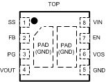
LMZ21701 SIL0008E_VIEW.gifFigure 1. LMZ21701 in the SIL0008E Package
SIL Package
8-Pin µSIP
Top View
LMZ21701 po_snvs853.gif

Pin Functions

PIN I/O DESCRIPTION
NAME NO.
SS 1 I Soft-start pin. An external capacitor connected to this pin sets the internal voltage reference ramp time. It can be used for tracking and sequencing.
FB 2 I Voltage feedback. Connect resistive voltage divider to this pin to set the output voltage.
PG 3 O Output power good (High = VOUT ready, Low = VOUT below nominal regulation); open drain (requires pull-up resistor; goes low impedance when EN is low).
VOUT 4 O Output Voltage. Connected to one terminal of the integrated inductor. Connect output filter capacitor between VOUT and PGND.
GND 5 I Ground for the power MOSFETs and gate-drive circuitry.
VOS 6 I Output voltage sense pin and connection for the control loop circuitry.
EN 7 I Enable input (High = enabled, Low = disabled). Internal pull down resistor keeps logic level low if pin is left floating.
VIN 8 I Supply voltage for control circuitry and power stage.
PAD Electrically connected to GND. Must be soldered to a ground copper plane to achieve appropriate power dissipation and mechanical reliability.