SNVS686K March   2011  – May 2024 LMZ22005

PRODUCTION DATA  

  1.   1
  2. Features
  3. Applications
  4. Description
  5. Pin Configuration and Functions
  6. Specifications
    1. 5.1 Absolute Maximum Ratings
    2. 5.2 ESD Ratings
    3. 5.3 Recommended Operating Conditions
    4. 5.4 Thermal Information
    5. 5.5 Electrical Characteristics
    6. 5.6 Typical Characteristics
  7. Detailed Description
    1. 6.1 Overview
    2. 6.2 Functional Block Diagram
    3. 6.3 Feature Description
      1. 6.3.1 Synchronization Input
      2. 6.3.2 Output Overvoltage Protection
      3. 6.3.3 Current Limit
      4. 6.3.4 Thermal Protection
      5. 6.3.5 Prebiased Start-Up
    4. 6.4 Device Functional Modes
      1. 6.4.1 Discontinuous And Continuous Conduction Modes
  8. Application and Implementation
    1. 7.1 Application Information
    2. 7.2 Typical Application
      1. 7.2.1 Design Requirements
      2. 7.2.2 Detailed Design Procedure
        1. 7.2.2.1 Design Steps
        2. 7.2.2.2 Enable Divider, RENT, RENB and RENH Selection
        3. 7.2.2.3 Output Voltage Selection
        4. 7.2.2.4 Soft-start Capacitor Selection
        5. 7.2.2.5 Tracking Supply Divider Option
        6. 7.2.2.6 CO Selection
        7. 7.2.2.7 CIN Selection
        8. 7.2.2.8 Discontinuous And Continuous Conduction Modes Selection
      3. 7.2.3 Application Curves
  9. Power Supply Recommendations
  10. Layout
    1. 9.1 Layout Guidelines
    2. 9.2 Layout Examples
    3. 9.3 Power Dissipation and Thermal Considerations
    4. 9.4 Power Module SMT Guidelines
  11. 10Device and Documentation Support
    1. 10.1 Device Support
      1. 10.1.1 Development Support
    2. 10.2 Documentation Support
      1. 10.2.1 Related Documentation
    3. 10.3 Support Resources
    4. 10.4 Trademarks
    5. 10.5 Electrostatic Discharge Caution
    6. 10.6 Glossary
  12. 11Revision History
  13. 12Mechanical, Packaging, and Orderable Information

Package Options

Mechanical Data (Package|Pins)
Thermal pad, mechanical data (Package|Pins)
Orderable Information

Discontinuous And Continuous Conduction Modes

At light load the regulator will operate in discontinuous conduction mode (DCM). With load currents above the critical conduction point, it will operate in continuous conduction mode (CCM). In CCM, current flows through the inductor through the entire switching cycle and never falls to zero during the OFF-time. When operating in DCM, inductor current is maintained to an average value equaling IOUT. Inductor current exhibits normal behavior for the emulated current mode control method used. Output voltage ripple typically increases during this mode of operation.

Figure 6-2 is a comparison pair of waveforms of the showing both CCM (upper) and DCM operating modes.
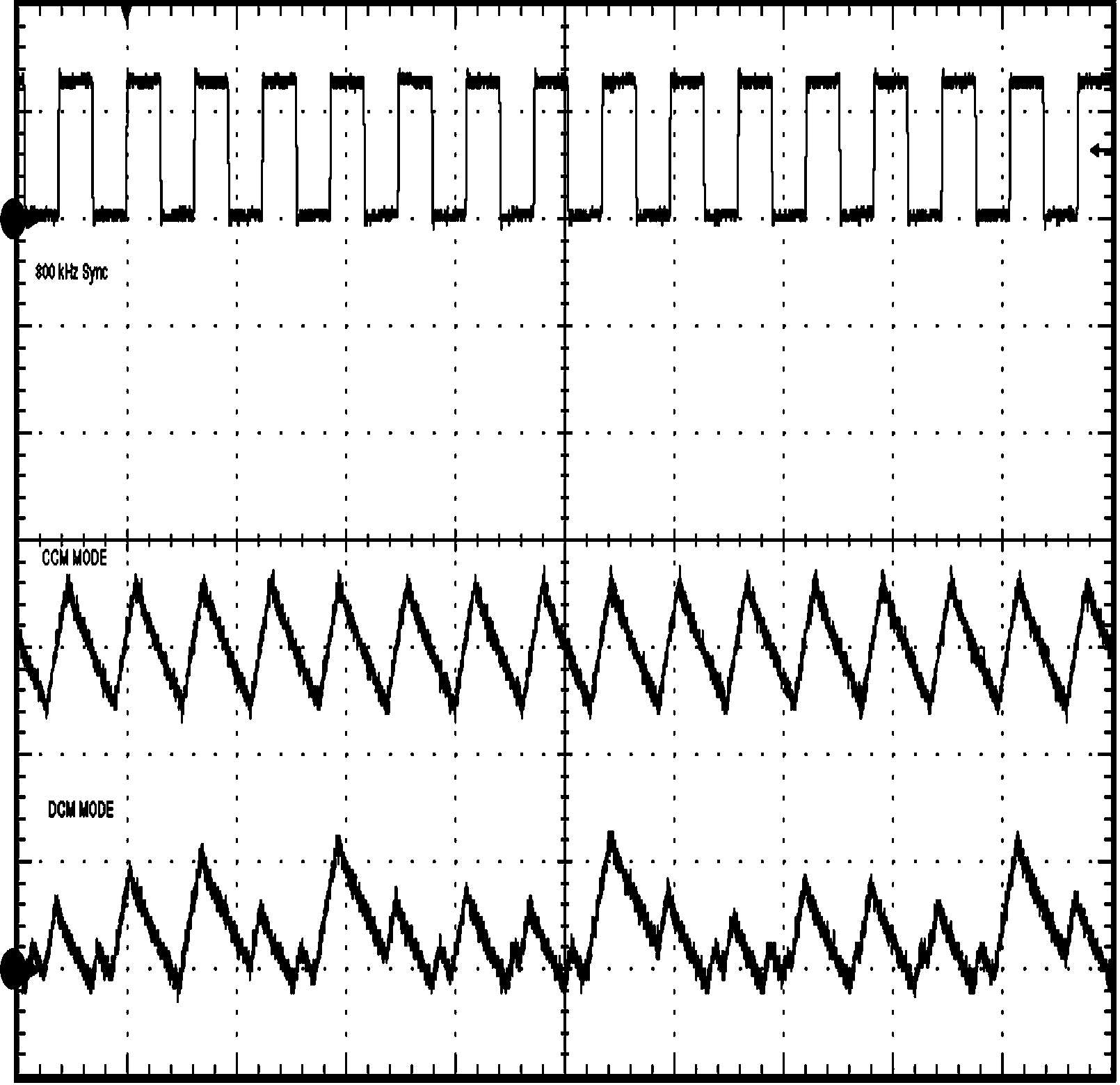
LMZ22005 CCM and DCM Operating Modes
VIN = 12 V, VO = 3.3 V, IO = 3 A / 0.3 A 2 μs/div
Figure 6-2 CCM and DCM Operating Modes