SNVS686K March 2011 – May 2024 LMZ22005
PRODUCTION DATA
- 1
- 1 Features
- 2 Applications
- 3 Description
- 4 Pin Configuration and Functions
- 5 Specifications
- 6 Detailed Description
- 7 Application and Implementation
- 8 Power Supply Recommendations
- 9 Layout
- 10Device and Documentation Support
- 11Revision History
- 12Mechanical, Packaging, and Orderable Information
Package Options
Mechanical Data (Package|Pins)
- NDW|7
Thermal pad, mechanical data (Package|Pins)
Orderable Information
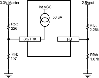
7.2.2.5 Tracking Supply Divider Option
The tracking function allows the module to be connected as a slave supply to a primary voltage rail (often the 3.3-V system rail) where the slave module output voltage is lower than that of the master. Proper configuration allows the slave rail to power up coincident with the master rail such that the voltage difference between the rails during ramp-up is small (that is, <0.15 V typical). The values for the tracking resistive divider must be selected such that the effect of the internal 50-µA current source is minimized. In most cases the ratio of the tracking divider resistors is the same as the ratio of the output voltage setting divider. Proper operation in tracking mode dictates the soft-start time of the slave rail be shorter than the master rail; a condition that is easy satisfy because the CSS cap is replaced by RTKB. The tracking function is only supported for the power up interval of the master supply; once the SS/TRK rises past 0.8V the input is no longer enabled and the 50-µA internal current source is switched off.
 Figure 7-3 Tracking Option Input Detail