SLVSBC7E October 2013 – September 2018 LMZ31530
PRODUCTION DATA.
- 1 Features
- 2 Applications
- 3 Description
- 4 Specifications
- 5 Device Information
- 6 Typical Characteristics (PVIN = VIN = 12 V)
- 7 Typical Characteristics (PVIN = VIN = 5 V)
-
8 Application Information
- 8.1 Adjusting the Output Voltage
- 8.2 Frequency Select
- 8.3 Capacitor Recommendations for the LMZ31530 Power Supply
- 8.4 Transient Response
- 8.5 Application Curves
- 8.6 Application Schematics
- 8.7 Custom Design With WEBENCH® Tools
- 8.8 VIN and PVIN Input Voltage
- 8.9 3.3 V PVIN Operation
- 8.10 Power Good (PWRGD)
- 8.11 Slow Start (SS_SEL)
- 8.12 Auto-Skip Eco-mode / Forced Continuous Conduction Mode
- 8.13 Power-Up Characteristics
- 8.14 Pre-Biased Start-Up
- 8.15 Remote Sense
- 8.16 Output On/Off Inhibit (INH)
- 8.17 Overcurrent Protection
- 8.18 Current Limit (ILIM) Adjust
- 8.19 Thermal Shutdown
- 8.20 Layout Considerations
- 8.21 EMI
- 9 Revision History
- 10Device and Documentation Support
- 11Mechanical, Packaging, and Orderable Information
Package Options
Refer to the PDF data sheet for device specific package drawings
Mechanical Data (Package|Pins)
- RLG|72
Thermal pad, mechanical data (Package|Pins)
Orderable Information
8.16 Output On/Off Inhibit (INH)
The INH pin provides electrical on/off control of the device. Once the INH pin voltage exceeds the threshold voltage, the device starts operation. If the INH pin voltage is pulled below the threshold voltage, the regulator stops switching and enters low quiescent current state.
The INH pin has an internal pull-up current source, allowing the user to float the INH pin for enabling the device. If an application requires controlling the INH pin, use an open drain/collector device, or a suitable logic gate to interface with the pin.
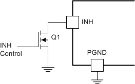
Figure 23 shows the typical application of the inhibit function. The Inhibit control has its own internal pull-up to VIN potential. An open-collector or open-drain device is recommended to control this input.
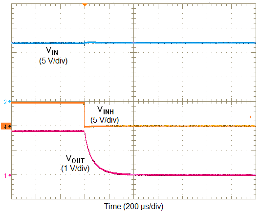
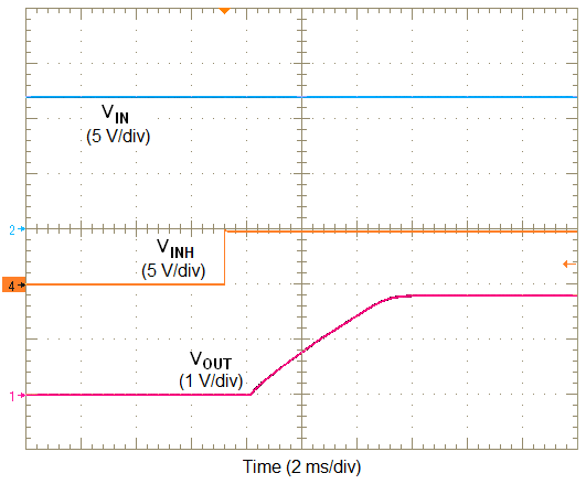
Turning Q1 on applies a low voltage to the inhibit control (INH) pin and disables the output of the supply, shown in Figure 24. If Q1 is turned off, the supply executes a soft-start power-up sequence, as shown in Figure 25. The waveforms were measured with a 12-A constant resistance load.
 Figure 23. Typical Inhibit Control
  Figure 24. Inhibit Turn-Off
  Figure 25. Inhibit Turn-On