SLVSBV8E June 2013 – February 2020 LMZ31704
PRODUCTION DATA.
- 1 Features
- 2 Applications
- 3 Description
- 4 Revision History
- 5 Specifications
- 6 Device Information
- 7 Typical Characteristics (PVIN = VIN = 12 V)
- 8 Typical Characteristics (PVIN = VIN = 5 V)
- 9 Typical Characteristics (PVIN = 3.3 V, VIN = 5 V)
-
10Application Information
- 10.1 Adjusting the Output Voltage
- 10.2 Capacitor Recommendations for the LMZ31704 Power Supply
- 10.3 Transient Response
- 10.4 Transient Waveforms
- 10.5 Application Schematics
- 10.6 Custom Design With WEBENCH® Tools
- 10.7 VIN and PVIN Input Voltage
- 10.8 3.3 V PVIN Operation
- 10.9 Power Good (PWRGD)
- 10.10 SYNC_OUT
- 10.11 Parallel Operation
- 10.12 Light Load Efficiency (LLE)
- 10.13 Power-Up Characteristics
- 10.14 Pre-Biased Start-up
- 10.15 Remote Sense
- 10.16 Thermal Shutdown
- 10.17 Output On/Off Inhibit (INH)
- 10.18 Slow Start (SS/TR)
- 10.19 Overcurrent Protection
- 10.20 Synchronization (CLK)
- 10.21 Sequencing (SS/TR)
- 10.22 Programmable Undervoltage Lockout (UVLO)
- 10.23 Layout Considerations
- 10.24 EMI
- 11Device and Documentation Support
- 12Mechanical, Packaging, and Orderable Information
Package Options
Mechanical Data (Package|Pins)
- RVQ|42
Thermal pad, mechanical data (Package|Pins)
Orderable Information
10.20 Synchronization (CLK)
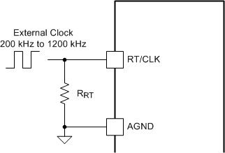
An internal phase locked loop (PLL) has been implemented to allow synchronization between 200 kHz and 1200 kHz, and to easily switch from RT mode to CLK mode. To implement the synchronization feature, connect a square wave clock signal to the RT/CLK pin with a duty cycle between 20% to 80%. The clock signal amplitude must transition lower than 0.5 V and higher than 2.0 V. The start of the switching cycle is synchronized to the falling edge of RT/CLK pin. In applications where both RT mode and CLK mode are needed, the device can be configured as shown in Figure 34.
Before the external clock is present, the device works in RT mode and the switching frequency is set by RT resistor. When the external clock is present, the CLK mode overrides the RT mode. The first time the CLK pin is pulled above the RT/CLK high threshold (2.0 V), the device switches from RT mode to CLK mode and the RT/CLK pin becomes high impedance as the PLL starts to lock onto the frequency of the external clock. It is not recommended to switch from CLK mode back to RT mode because the internal switching frequency drops to 100 kHz first before returning to the switching frequency set by the RT resistor (RRT).
 Figure 34. RT/CLK Configuration
 The switching frequency must be selected based on the output voltages of the devices being synchronized. shows the allowable frequencies for a given range of output voltages. The allowable switching frequency changes based on the maximum output current (IOUT) of an application. The table shows the VOUT range when IOUT ≤ 4 A, 3 A, and 2 A. For the most efficient solution, always synchronize to the lowest allowable frequency. For example, an application requires synchronizing three LMZ31704 devices with output voltages of 1.0 V, 1.2 V, and 1.8 V, all powered from PVIN = 12 V. Table 7 shows that all three output voltages should be synchronized to 300 kHz.
Table 7. Allowable Switching Frequency versus Output Voltage
| SWITCHING FREQUENCY (kHz) | PVIN = 12 V | PVIN = 5 V | ||||
|---|---|---|---|---|---|---|
| VOUT RANGE (V) | VOUT RANGE (V) | |||||
| IOUT ≤ 4 A | IOUT ≤ 3 A | IOUT ≤ 2 A | IOUT ≤ 4 A | IOUT ≤ 3 A | IOUT ≤ 2 A | |
| 200 | 0.6 - 1.2 | 0.6 - 1.6 | 0.6 - 2.0 | 0.6 - 4.3 | 0.6 - 4.3 | 0.6 - 4.2 |
| 300 | 0.8 - 1.8 | 0.8 - 2.6 | 0.8 - 3.5 | 0.6 - 4.3 | 0.6 - 4.3 | 0.6 - 4.2 |
| 400 | 1.1 - 2.7 | 1.1 - 4.1 | 1.1 - 5.5 | 0.6 - 4.3 | 0.6 - 4.3 | 0.6 - 4.2 |
| 500 | 1.3 - 3.9 | 1.3 - 5.5 | 1.3 - 5.5 | 0.6 - 4.3 | 0.6 - 4.3 | 0.6 - 4.2 |
| 600 | 1.6 - 5.5 | 1.6 - 5.5 | 1.6 - 5.5 | 0.8 - 4.3 | 0.8 - 4.3 | 0.6 - 4.2 |
| 700 | 1.9 - 5.5 | 1.9 - 5.5 | 1.9 - 5.5 | 0.8 - 4.2 | 0.8 - 4.2 | 0.8 - 4.2 |
| 800 | 2.1 - 5.5 | 2.1 - 5.5 | 2.1 - 5.5 | 0.9 - 4.1 | 0.9 - 4.1 | 0.8 - 4.1 |
| 900 | 2.4 - 5.5 | 2.4 - 5.5 | 2.4 - 5.5 | 1.0 - 4.0 | 1.0 - 4.0 | 0.9 - 4.0 |
| 1000 | 2.6 - 5.5 | 2.6 - 5.5 | 2.6 - 5.5 | 1.1 - 3.9 | 1.1 - 3.9 | 1.0 - 3.9 |
| 1100 | 2.9 - 5.5 | 2.9 - 5.5 | 2.9 - 5.5 | 1.2 - 3.8 | 1.2 - 3.8 | 1.1 - 3.8 |
| 1200 | 3.2 - 5.5 | 3.2 - 5.5 | 3.2 - 5.5 | 1.5 - 3.7 | 1.5 - 3.7 | 1.2 - 3.7 |