SNVSAO6C September   2017  – March 2018 LMZM33603

PRODUCTION DATA.  

  1. Features
  2. Applications
    1.     Simplified Schematic
  3. Description
    1.     Safe Operating Area
  4. Revision History
  5. Pin Configuration and Functions
    1.     Pin Functions
  6. Specifications
    1. 6.1 Absolute Maximum Ratings
    2. 6.2 ESD Ratings
    3. 6.3 Recommended Operating Conditions
    4. 6.4 Thermal Information
    5. 6.5 Electrical Characteristics
    6. 6.6 Switching Characteristics
    7. 6.7 Typical Characteristics (VIN = 5 V)
    8. 6.8 Typical Characteristics (VIN = 12 V)
    9. 6.9 Typical Characteristics (VIN = 24 V)
  7. Detailed Description
    1. 7.1 Overview
    2. 7.2 Functional Block Diagram
    3. 7.3 Feature Description
      1. 7.3.1  Adjusting the Output Voltage
      2. 7.3.2  Feed-Forward Capacitor, CFF
      3. 7.3.3  Output Current vs Output Voltage
      4. 7.3.4  Voltage Dropout
      5. 7.3.5  Switching Frequency (RT)
      6. 7.3.6  Synchronization (SYNC)
      7. 7.3.7  Input Capacitors
      8. 7.3.8  Output Capacitors
      9. 7.3.9  Output On/Off Enable (EN)
      10. 7.3.10 Programmable Undervoltage Lockout (UVLO)
      11. 7.3.11 Power Good (PGOOD)
      12. 7.3.12 Overcurrent Protection (OCP)
      13. 7.3.13 Thermal Shutdown
    4. 7.4 Device Functional Modes
      1. 7.4.1 Active Mode
      2. 7.4.2 Shutdown Mode
  8. Application and Implementation
    1. 8.1 Application Information
    2. 8.2 Typical Application
      1. 8.2.1 Design Requirements
      2. 8.2.2 Detailed Design Procedure
        1. 8.2.2.1 Custom Design With WEBENCH® Tools
        2. 8.2.2.2 Output Voltage Setpoint
        3. 8.2.2.3 Feed-Forward Capacitor (CFF)
        4. 8.2.2.4 Setting the Switching Frequency
        5. 8.2.2.5 Input Capacitors
        6. 8.2.2.6 Output Capacitor Selection
        7. 8.2.2.7 Application Curves
  9. Power Supply Recommendations
  10. 10Layout
    1. 10.1 Layout Guidelines
    2. 10.2 Layout Examples
    3. 10.3 Theta JA vs PCB Area
    4. 10.4 EMI
      1. 10.4.1 EMI Plots
    5. 10.5 Package Specifications
  11. 11Device and Documentation Support
    1. 11.1 Device Support
      1. 11.1.1 Third-Party Products Disclaimer
      2. 11.1.2 Custom Design With WEBENCH® Tools
    2. 11.2 Related Documentation
    3. 11.3 Receiving Notification of Documentation Updates
    4. 11.4 Community Resources
    5. 11.5 Trademarks
    6. 11.6 Electrostatic Discharge Caution
    7. 11.7 Glossary
  12. 12Mechanical, Packaging, and Orderable Information
    1. 12.1 Tape and Reel Information

Package Options

Mechanical Data (Package|Pins)
Thermal pad, mechanical data (Package|Pins)
Orderable Information

Layout Examples

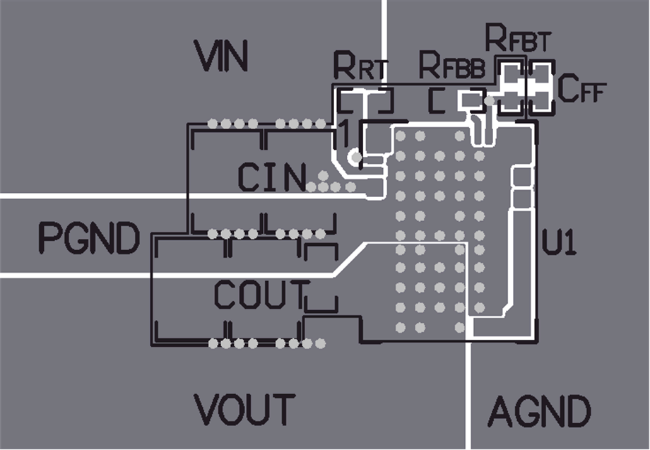
LMZM33603 TopLayer2.gifFigure 38. Typical Top-Layer Layout
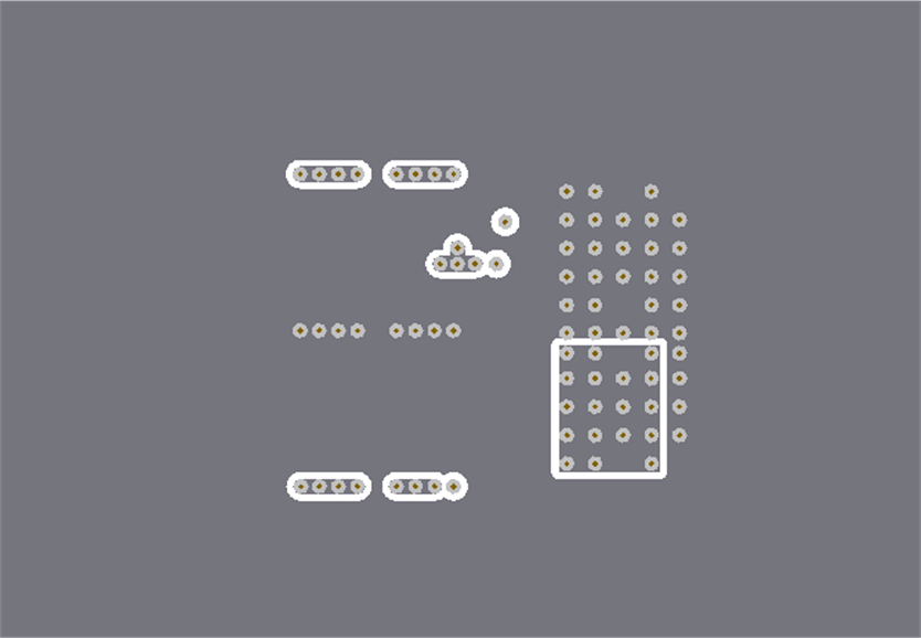
LMZM33603 BotLayer.gifFigure 40. Typical Layer 3 Layout
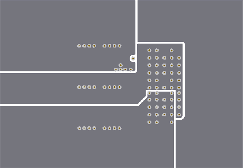
LMZM33603 RecLayer2.gifFigure 39. Typical Layer-2 Layout
LMZM33603 BotLayer.gifFigure 41. Typical Bottom-Layer Layout