SNVSAO6C September 2017 – March 2018 LMZM33603
PRODUCTION DATA.
- 1 Features
- 2 Applications
- 3 Description
- 4 Revision History
- 5 Pin Configuration and Functions
- 6 Specifications
-
7 Detailed Description
- 7.1 Overview
- 7.2 Functional Block Diagram
- 7.3
Feature Description
- 7.3.1 Adjusting the Output Voltage
- 7.3.2 Feed-Forward Capacitor, CFF
- 7.3.3 Output Current vs Output Voltage
- 7.3.4 Voltage Dropout
- 7.3.5 Switching Frequency (RT)
- 7.3.6 Synchronization (SYNC)
- 7.3.7 Input Capacitors
- 7.3.8 Output Capacitors
- 7.3.9 Output On/Off Enable (EN)
- 7.3.10 Programmable Undervoltage Lockout (UVLO)
- 7.3.11 Power Good (PGOOD)
- 7.3.12 Overcurrent Protection (OCP)
- 7.3.13 Thermal Shutdown
- 7.4 Device Functional Modes
- 8 Application and Implementation
- 9 Power Supply Recommendations
- 10Layout
- 11Device and Documentation Support
- 12Mechanical, Packaging, and Orderable Information
Package Options
Mechanical Data (Package|Pins)
- RLR|18
Thermal pad, mechanical data (Package|Pins)
Orderable Information
7.3.6 Synchronization (SYNC)
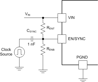
The LMZM33603 switching frequency can also be synchronized to an external clock from 200 kHz to 1.2 MHz. To implement the synchronization feature, couple an AC signal to the EN/SYNC pin (pin 2) with a peak-to-peak amplitude of at least 2.8 V, not to exceed 5.5 V. The minimum SYNC clock ON and OFF time must be longer than 100ns. The AC signal must be coupled through a small capacitor (1 nF) as shown in Figure 26. RENT is required for this synchronization circuit, but RENB is not required if an external UVLO adjustment is not needed.
Before the external clock is present, or when a valid clock signal is removed, the device works in RT mode and the switching frequency is set by RRT resistor. Select RRT so that it sets the frequency close to the external synchronization frequency. When the external clock is present, the SYNC mode overrides the RT mode.
The synchronization frequency must be selected based on the output voltages of the devices being synchronized. Table 3 and Table 4 show the allowable frequencies for a given range of output voltages. For the most efficient solution, always select the lowest allowable frequency.
 Figure 26. AC-Coupled SYNC Signal